MOD5272-100IR NetBurner Inc, MOD5272-100IR Datasheet - Page 168
MOD5272-100IR
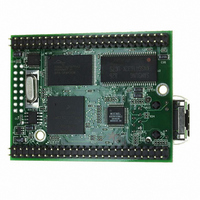
Manufacturer Part Number
MOD5272-100IR
Description
PROCESSOR MODULE FLASH MOD5272
Manufacturer
NetBurner Inc
Type
Controllers & Processorsr
Datasheets
1.MOD5272-100IR.pdf
(2 pages)
2.MOD5272-100IR.pdf
(3 pages)
3.MOD5272-100IR.pdf
(550 pages)
Specifications of MOD5272-100IR
Module/board Type
Processor Module
Ethernet Connection Type
10/100 Ethernet Port RJ-45
Operating Voltage
3.3 V
Product
Modules
Lead Free Status / RoHS Status
Lead free / RoHS Compliant
For Use With/related Products
MOD5272
For Use With
528-1001 - KIT DEVELOP NETWORK FOR MOD5272
Lead Free Status / Rohs Status
Lead free / RoHS Compliant
Other names
528-1008


Programming Model
6.2.2 Module Base Address Register (MBAR)
The supervisor-level MBAR, Figure 6-2, specifies the base address and allowable access
types for all internal peripherals. It is written with a MOVEC instruction using the CPU
address 0xC0F. (See the ColdFire Family Programmer’s Reference Manual.) MBAR can
be read or written through the debug module as a read/write register, as described in.” Once
MBAR has been initialized, it can be read and written in supervisor mode at the address
programmed into the base address (BA) field.
The valid bit, MBAR[V], is cleared at system reset to prevent incorrect references before
MBAR is written; other MBAR bits are uninitialized at reset. To access internal peripherals,
write MBAR with the appropriate base address (BA) and set MBAR[V] after system reset.
All internal peripheral registers occupy a single relocatable memory block along 64-Kbyte
boundaries. If MBAR[V] is set, MBAR[BA] is compared to the upper 16 bits of the full
32-bit internal address to determine if an internal peripheral is being accessed. MBAR
masks specific address spaces using the address space fields. Attempts to access a masked
address space generate an external bus access.
Addresses hitting overlapping memory spaces take the following priority:
Thus, if an overlapping address hits in the SRAM, ROM, or cache, the SIM will not
generate a bus cycle, either externally or to an on-chip peripheral.
Table 6-2 describes MBAR fields.
6-4
Address
Reset
1. SRAM, ROM, and cache
2. MBAR
3. Chip select
Field
R/W
31
The MBAR region must be mapped to non-cacheable space.
Figure 6-2. Module Base Address Register (MBAR)
W initially through MOVEC; R/W after initialization in supervisor mode
BA
CPU + 0x0C0F initially; MBAR+0x000 after initialization
MCF5272 User’s Manual
NOTE:
16 15
Undefined
—
5
SC SD UC UD V
4
Attribute Mask Bits
3
MOTOROLA
2
1
0
0
Related parts for MOD5272-100IR
Image
Part Number
Description
Manufacturer
Datasheet
Request
R

Part Number:
Description:
Ethernet Modules & Development Tools MOD5272 Processor Board
Manufacturer:
NetBurner Inc
Datasheet:
Part Number:
Description:
Ethernet Modules & Development Tools MOD5272 Industrial Temperature
Manufacturer:
NetBurner Inc
Part Number:
Description:
Ethernet Modules & Development Tools MOD5272 MODULE
Manufacturer:
NetBurner Inc
Datasheet:

Part Number:
Description:
PROCESSOR MODULE FLASH
Manufacturer:
NetBurner Inc
Datasheet:

Part Number:
Description:
Ethernet Modules & Development Tools 32Bit 62MHz Core Module 50Pin DIP
Manufacturer:
NetBurner Inc
Datasheet:

Part Number:
Description:
BOARD SERIAL-ETHERNET 512K FLASH
Manufacturer:
NetBurner Inc
Datasheet:

Part Number:
Description:
PROCESSOR MODULE 512KB FLASH
Manufacturer:
NetBurner Inc
Datasheet:

Part Number:
Description:
DUAL PORT SERIAL-ETHERNET
Manufacturer:
NetBurner Inc
Datasheet:

Part Number:
Description:
PROCESSOR MODULE 512KB FLASH
Manufacturer:
NetBurner Inc
Datasheet:

Part Number:
Description:
MOD5234 10/100 ETHERNET MODULE
Manufacturer:
NetBurner Inc
Datasheet:

Part Number:
Description:
KIT DEVELOP NETWORK FOR MOD5282
Manufacturer:
NetBurner Inc
Datasheet:

Part Number:
Description:
KIT DEVELOP NETWORK FOR MOD5272
Manufacturer:
NetBurner Inc
Datasheet:

Part Number:
Description:
Ethernet ICs 32bit 147MHz CAN-to- Ethnt Device IndTemp
Manufacturer:
NetBurner Inc
Datasheet: