MOD5272-100IR NetBurner Inc, MOD5272-100IR Datasheet - Page 295
MOD5272-100IR
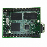
Manufacturer Part Number
MOD5272-100IR
Description
PROCESSOR MODULE FLASH MOD5272
Manufacturer
NetBurner Inc
Type
Controllers & Processorsr
Datasheets
1.MOD5272-100IR.pdf
(2 pages)
2.MOD5272-100IR.pdf
(3 pages)
3.MOD5272-100IR.pdf
(550 pages)
Specifications of MOD5272-100IR
Module/board Type
Processor Module
Ethernet Connection Type
10/100 Ethernet Port RJ-45
Operating Voltage
3.3 V
Product
Modules
Lead Free Status / RoHS Status
Lead free / RoHS Compliant
For Use With/related Products
MOD5272
For Use With
528-1001 - KIT DEVELOP NETWORK FOR MOD5272
Lead Free Status / Rohs Status
Lead free / RoHS Compliant
Other names
528-1008


MOTOROLA
The most important considerations for PCB layout deal with noise: noise on the power
supply, noise generated by the digital circuitry on the device, and noise resulting from
coupling digital signals into the analog signals. The best PCB layout methods to prevent
noise–induced problems are as follows:
12.5.3 Recommended USB Protection Circuit
Figure 12-25 shows the recommended external ESD protection circuit for the USB.
• Keep digital signals as far away from analog signals (D+ and D-) as possible.
• Use short, low inductance traces for the analog circuitry to reduce inductive,
• Use short, low inductance traces for digital circuitry to reduce inductive, capacitive,
• Bypass capacitors should be connected between the Vdd and GND pairs with
• Use short, wide, low inductance traces to connect all of the GND pins together and,
• Use short, wide, low inductance traces to connect all of the Vdd power supply pins
• The 48-MHz oscillator must be located as close as possible to the chip package. This
capacitive, and radio frequency noise sensitivities.
and radio frequency radiated noise.
minimal trace length. These capacitors help supply the instantaneous currents of the
digital circuitry, in addition to decoupling the noise that may be generated by other
sections of the device or other circuitry on the power supply.
with a single trace, connect all of the GND pins to the power supply ground. This
helps to reduce voltage spikes in the ground circuit caused by high-speed digital
current spikes. Suppressing these voltage spikes on the integrated circuit is the
reason for multiple GND leads. A PCB with a ground plane connecting all of the
digital and analog GND pins together is the optimal ground configuration,
producing the lowest resistance and inductance in the ground circuit.
together and, with a single trace, connect all of the Vdd pins to the 3.3V power
supply. Connecting all of the digital and analog Vdd pins to the power plane would
be the optimal power distribution method for a multi-layer PCB with a power plane.
is required to minimize parasitic capacitance between crystal traces and ground.
Chapter 12. Universal Serial Bus (USB)
Line Interface
12-35
Related parts for MOD5272-100IR
Image
Part Number
Description
Manufacturer
Datasheet
Request
R

Part Number:
Description:
Ethernet Modules & Development Tools MOD5272 Processor Board
Manufacturer:
NetBurner Inc
Datasheet:
Part Number:
Description:
Ethernet Modules & Development Tools MOD5272 Industrial Temperature
Manufacturer:
NetBurner Inc
Part Number:
Description:
Ethernet Modules & Development Tools MOD5272 MODULE
Manufacturer:
NetBurner Inc
Datasheet:

Part Number:
Description:
PROCESSOR MODULE FLASH
Manufacturer:
NetBurner Inc
Datasheet:

Part Number:
Description:
Ethernet Modules & Development Tools 32Bit 62MHz Core Module 50Pin DIP
Manufacturer:
NetBurner Inc
Datasheet:

Part Number:
Description:
BOARD SERIAL-ETHERNET 512K FLASH
Manufacturer:
NetBurner Inc
Datasheet:

Part Number:
Description:
PROCESSOR MODULE 512KB FLASH
Manufacturer:
NetBurner Inc
Datasheet:

Part Number:
Description:
DUAL PORT SERIAL-ETHERNET
Manufacturer:
NetBurner Inc
Datasheet:

Part Number:
Description:
PROCESSOR MODULE 512KB FLASH
Manufacturer:
NetBurner Inc
Datasheet:

Part Number:
Description:
MOD5234 10/100 ETHERNET MODULE
Manufacturer:
NetBurner Inc
Datasheet:

Part Number:
Description:
KIT DEVELOP NETWORK FOR MOD5282
Manufacturer:
NetBurner Inc
Datasheet:

Part Number:
Description:
KIT DEVELOP NETWORK FOR MOD5272
Manufacturer:
NetBurner Inc
Datasheet:

Part Number:
Description:
Ethernet ICs 32bit 147MHz CAN-to- Ethnt Device IndTemp
Manufacturer:
NetBurner Inc
Datasheet: