MOD5272-100IR NetBurner Inc, MOD5272-100IR Datasheet - Page 36
MOD5272-100IR
Manufacturer Part Number
MOD5272-100IR
Description
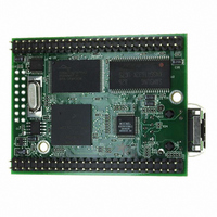
PROCESSOR MODULE FLASH MOD5272
Manufacturer
NetBurner Inc
Type
Controllers & Processorsr
Datasheets
1.MOD5272-100IR.pdf
(2 pages)
2.MOD5272-100IR.pdf
(3 pages)
3.MOD5272-100IR.pdf
(550 pages)
Specifications of MOD5272-100IR
Module/board Type
Processor Module
Ethernet Connection Type
10/100 Ethernet Port RJ-45
Operating Voltage
3.3 V
Product
Modules
Lead Free Status / RoHS Status
Lead free / RoHS Compliant
For Use With/related Products
MOD5272
For Use With
528-1001 - KIT DEVELOP NETWORK FOR MOD5272
Lead Free Status / Rohs Status
Lead free / RoHS Compliant
Other names
528-1008


19-3
19-4
19-5
19-6
19-7
19-8
19-9
19-10
20-1
20-2
20-3
20-4
20-5
20-6
20-7
21-1
21-2
23-1
23-2
23-3
23-4
23-5
23-6
23-7
23-8
23-9
23-10
23-11
23-12
23-13
23-14
23-15
23-16
23-17
23-18
23-19
23-20
23-21
23-22
23-23
23-24
23-25
A-1
Table
Number
xxxvi
Byte Strobe Operation for 32-Bit Data Bus.............................................................. 19-20
Connecting BS[3:0] to DQMx .................................................................................. 19-21
Processor Status Encoding........................................................................................ 19-38
MCF5272 Bus Width Selection ................................................................................ 19-39
MCF5272 CS0 Memory Bus Width Selection ......................................................... 19-39
MCF5272 High Impedance Mode Selection ............................................................ 19-39
Chip Select Memory Address Decoding Priority ....................................................... 20-4
Byte Strobe Operation for 32-Bit Data Bus................................................................ 20-6
Data Bus Requirement for Read/Write Cycles ........................................................... 20-8
External Bus Interface Codes for CSBRs ................................................................... 20-8
JTAG Signals .............................................................................................................. 21-3
Instructions.................................................................................................................. 21-7
Maximum Supply, Input Voltage and Storage Temperature ...................................... 23-1
Operating Temperature ............................................................................................... 23-2
Thermal Resistance..................................................................................................... 23-2
I/O Driver Capability .................................................................................................. 23-3
Clock Input and Output Timing Specifications .......................................................... 23-5
Processor Bus Input Timing Specifications................................................................ 23-6
Processor Bus Output Timing Specifications ............................................................. 23-8
Debug AC Timing Specification .............................................................................. 23-12
SDRAM Interface Timing Specifications................................................................. 23-13
MII Receive Signal Timing ...................................................................................... 23-15
MII Transmit Signal Timing..................................................................................... 23-16
MII Async Inputs Signal Timing .............................................................................. 23-17
MII Serial Management Channel Timing ................................................................. 23-17
Timer Module AC Timing Specifications ................................................................ 23-18
UART Modules AC Timing Specifications.............................................................. 23-19
IDL Master Mode Timing, PLIC Ports 1, 2, and 3 ................................................... 23-20
IDL Slave Mode Timing, PLIC Ports 0–3 ................................................................ 23-21
GCI Slave Mode Timing, PLIC Ports 0–3................................................................ 23-22
GCI Master Mode Timing, PLIC PORTs 1, 2, 3 ...................................................... 23-23
General-Purpose I/O Port AC Timing Specifications............................................... 23-25
USB Interface AC Timing Specifications................................................................. 23-25
IEEE 1149.1 (JTAG) AC Timing Specifications ..................................................... 23-26
QSPI Modules AC Timing Specifications................................................................ 23-28
PWM Modules AC Timing Specifications ............................................................... 23-28
On-Chip Module Base Address Offsets from MBAR ................................................. A-1
Byte Strobe Operation for 16-Bit Data Bus—SRAM Cycles.................................. 19-20
Byte Strobe Operation for 16-Bit Data Bus—SDRAM Cycles............................... 19-20
ColdFire Bus Signal Summary .................................................................................. 20-1
Byte Strobe Operation for 16-Bit Data Bus—SRAM Cycles.................................... 20-7
Byte Strobe Operation for 16-Bit Data Bus—SDRAM Cycles................................. 20-7
DC Electrical Specifications ...................................................................................... 23-3
MCF5272 User’s Manual
TABLES
Title
MOTOROLA
Number
Page
Related parts for MOD5272-100IR
Image
Part Number
Description
Manufacturer
Datasheet
Request
R

Part Number:
Description:
Ethernet Modules & Development Tools MOD5272 Processor Board
Manufacturer:
NetBurner Inc
Datasheet:
Part Number:
Description:
Ethernet Modules & Development Tools MOD5272 Industrial Temperature
Manufacturer:
NetBurner Inc
Part Number:
Description:
Ethernet Modules & Development Tools MOD5272 MODULE
Manufacturer:
NetBurner Inc
Datasheet:

Part Number:
Description:
PROCESSOR MODULE FLASH
Manufacturer:
NetBurner Inc
Datasheet:

Part Number:
Description:
Ethernet Modules & Development Tools 32Bit 62MHz Core Module 50Pin DIP
Manufacturer:
NetBurner Inc
Datasheet:

Part Number:
Description:
BOARD SERIAL-ETHERNET 512K FLASH
Manufacturer:
NetBurner Inc
Datasheet:

Part Number:
Description:
PROCESSOR MODULE 512KB FLASH
Manufacturer:
NetBurner Inc
Datasheet:

Part Number:
Description:
DUAL PORT SERIAL-ETHERNET
Manufacturer:
NetBurner Inc
Datasheet:

Part Number:
Description:
PROCESSOR MODULE 512KB FLASH
Manufacturer:
NetBurner Inc
Datasheet:

Part Number:
Description:
MOD5234 10/100 ETHERNET MODULE
Manufacturer:
NetBurner Inc
Datasheet:

Part Number:
Description:
KIT DEVELOP NETWORK FOR MOD5282
Manufacturer:
NetBurner Inc
Datasheet:

Part Number:
Description:
KIT DEVELOP NETWORK FOR MOD5272
Manufacturer:
NetBurner Inc
Datasheet:

Part Number:
Description:
Ethernet ICs 32bit 147MHz CAN-to- Ethnt Device IndTemp
Manufacturer:
NetBurner Inc
Datasheet: