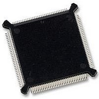
MC68331CEH25 Freescale Semiconductor, MC68331CEH25 Datasheet - Page 94

MC68331CEH25
Manufacturer Part Number
MC68331CEH25
Description
IC MCU 32BIT 25MHZ 132-PQFP
Manufacturer
Freescale Semiconductor
Series
M683xxr
Specifications of MC68331CEH25
Core Processor
CPU32
Core Size
32-Bit
Speed
25MHz
Connectivity
EBI/EMI, SCI, SPI, UART/USART
Peripherals
POR, PWM, WDT
Number Of I /o
18
Program Memory Type
ROMless
Voltage - Supply (vcc/vdd)
4.5 V ~ 5.5 V
Oscillator Type
Internal
Operating Temperature
-40°C ~ 85°C
Package / Case
132-QFP
Controller Family/series
68K
No. Of I/o's
18
Cpu Speed
25MHz
No. Of Timers
1
Embedded Interface Type
QSPI, SCI, UART
No. Of Pwm Channels
2
Digital Ic Case Style
PQFP
Rohs Compliant
Yes
Processor Series
M683xx
Core
CPU32
Data Bus Width
32 bit
Data Ram Size
80 B
Interface Type
QSPI, SCI, UART
Maximum Clock Frequency
25 MHz
Number Of Programmable I/os
18
Number Of Timers
1
Maximum Operating Temperature
+ 85 C
Mounting Style
SMD/SMT
Minimum Operating Temperature
- 40 C
Eeprom Size
-
Ram Size
-
Program Memory Size
-
Data Converters
-
Lead Free Status / Rohs Status
Details
Available stocks
Company
Part Number
Manufacturer
Quantity
Price
Company:
Part Number:
MC68331CEH25
Manufacturer:
PANASONIC
Quantity:
2 000
Company:
Part Number:
MC68331CEH25
Manufacturer:
Freescale Semiconductor
Quantity:
135
Company:
Part Number:
MC68331CEH25
Manufacturer:
Freescale Semiconductor
Quantity:
10 000
4
4.8.1.2 Chip-Select Base Address Registers
4.8.1.3 Chip-Select Option Registers
4-52
A pin programmed as a discrete output drives an external signal to the value specified
in the pin data register. No discrete output function is available on pins CSBOOT, BR,
BG, or BGACK. ADDR23 provides ECLK output rather than a discrete output signal.
When a pin is programmed for discrete output or alternate function, internal chip-select
logic still functions and can be used to generate DSACK or AVEC internally on an ad-
dress and control signal match.
Each chip select has an associated base address register. A base address is the low-
est address in the block of addresses enabled by a chip select. Block size is the extent
of the address block above the base address. Block size is determined by the value
contained in a BLKSZ field. Block addresses for different chip selects can overlap.
The BLKSZ field determines which bits in the base address field are compared to cor-
responding bits on the address bus during an access. Provided other constraints de-
termined by option register fields are also satisfied, when a match occurs, the
associated chip-select signal is asserted. Table 4-21 shows BLKSZ encoding.
The chip-select address compare logic uses only the most significant bits to match an
address within a block. The value of the base address must be a multiple of block size.
Base address register diagrams show how base register bits correspond to address
lines.
After reset, the MCU fetches the initialization routine from the address contained in the
reset vector, located beginning at address $000000 of program space. To support
bootstrap operation from reset, the base address field in chip-select base address reg-
ister boot (CSBARBT) has a reset value of all zeros. A memory device containing the
reset vector and initialization routine can be automatically enabled by CSBOOT after
a reset. The block size field in CSBARBT has a reset value of 512 Kbytes. Refer to
4.8.4 Chip-Select Reset Operation for more information.
Option register fields determine timing of and conditions for assertion of chip-select
signals. To assert a chip-select signal, and to provide DSACK or autovector support,
other constraints set by fields in the option register and in the base address register
must also be satisfied. Table 4-22 is a summary of option register functions.
BLKSZ[2:0]
000
001
010
011
100
101
110
111
Freescale Semiconductor, Inc.
For More Information On This Product,
Table 4-21 Block Size Encoding
SYSTEM INTEGRATION MODULE
Go to: www.freescale.com
Block Size
128 Kbyte
256 Kbyte
512 Kbyte
16 Kbyte
64 Kbyte
1 Mbyte
2 Kbyte
8 Kbyte
Address Lines Compared
ADDR[23:11]
ADDR[23:13]
ADDR[23:14]
ADDR[23:16]
ADDR[23:17]
ADDR[23:18]
ADDR[23:19]
ADDR[23:20]
USER’S MANUAL
MC68331


