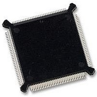
MC68331CEH25 Freescale Semiconductor, MC68331CEH25 Datasheet - Page 66

MC68331CEH25
Manufacturer Part Number
MC68331CEH25
Description
IC MCU 32BIT 25MHZ 132-PQFP
Manufacturer
Freescale Semiconductor
Series
M683xxr
Specifications of MC68331CEH25
Core Processor
CPU32
Core Size
32-Bit
Speed
25MHz
Connectivity
EBI/EMI, SCI, SPI, UART/USART
Peripherals
POR, PWM, WDT
Number Of I /o
18
Program Memory Type
ROMless
Voltage - Supply (vcc/vdd)
4.5 V ~ 5.5 V
Oscillator Type
Internal
Operating Temperature
-40°C ~ 85°C
Package / Case
132-QFP
Controller Family/series
68K
No. Of I/o's
18
Cpu Speed
25MHz
No. Of Timers
1
Embedded Interface Type
QSPI, SCI, UART
No. Of Pwm Channels
2
Digital Ic Case Style
PQFP
Rohs Compliant
Yes
Processor Series
M683xx
Core
CPU32
Data Bus Width
32 bit
Data Ram Size
80 B
Interface Type
QSPI, SCI, UART
Maximum Clock Frequency
25 MHz
Number Of Programmable I/os
18
Number Of Timers
1
Maximum Operating Temperature
+ 85 C
Mounting Style
SMD/SMT
Minimum Operating Temperature
- 40 C
Eeprom Size
-
Ram Size
-
Program Memory Size
-
Data Converters
-
Lead Free Status / Rohs Status
Details
Available stocks
Company
Part Number
Manufacturer
Quantity
Price
Company:
Part Number:
MC68331CEH25
Manufacturer:
PANASONIC
Quantity:
2 000
Company:
Part Number:
MC68331CEH25
Manufacturer:
Freescale Semiconductor
Quantity:
135
Company:
Part Number:
MC68331CEH25
Manufacturer:
Freescale Semiconductor
Quantity:
10 000
- Current page: 66 of 254
- Download datasheet (7Mb)
4
4.5.2.1 Read Cycle
4-24
the cycle is terminated with DSACK, the MCU inserts wait cycles in clock period incre-
ments until either DSACK signal goes low.
If no peripheral responds to an access, or if an access is invalid, external logic should
assert the BERR or HALT signals to abort the bus cycle (when BERR and HALT are
asserted simultaneously, the CPU32 acts as though only BERR is asserted). If bus ter-
mination signals are not asserted within a specified period, the bus monitor terminates
the cycle.
During a read cycle, the MCU transfers data from an external memory or peripheral
device. If the instruction specifies a long-word or word operation, the MCU attempts to
read two bytes at once. For a byte operation, the MCU reads one byte. The portion of
the data bus from which each byte is read depends on operand size, peripheral ad-
dress, and peripheral port size. Figure 4-9 is a flowchart of a word read cycle. Refer
to 4.4.2 Dynamic Bus Sizing, 4.4.4 Misaligned Operands, and the SIM Reference
Manual (SIMRM/AD) for more information.
2) DRIVE ADDRESS ON ADDR[23:0]
3) DRIVE FUNCTION CODE ON FC[2:0]
4) DRIVE SIZ[1:0] FOR OPERAND SIZE
1) SET R/W TO READ
The SIM bus monitor asserts BERR when response time exceeds a
predetermined limit. Bus monitor period is determined by the BMT
field in SYPCR. The bus monitor cannot be disabled; maximum mon-
itor period is 64 system clock cycles.
NEGATE AS AND DS (S5)
START NEXT CYCLE (S0)
ASSERT AS AND DS (S1)
ADDRESS DEVICE (S0)
DECODE DSACK (S3)
LATCH DATA (S4)
MCU
Figure 4-9 Word Read Cycle Flowchart
Freescale Semiconductor, Inc.
For More Information On This Product,
SYSTEM INTEGRATION MODULE
Go to: www.freescale.com
NOTE
1) DECODE ADDR, R/W, SIZ[1:0], DS
2) PLACE DATA ON DATA[15:0] OR
3) DRIVE DSACK SIGNALS
1) REMOVE DATA FROM DATA BUS
2) NEGATE DSACK
DATA[15:8] IF 8-BIT DATA
TERMINATE CYCLE (S5)
PRESENT DATA (S2)
PERIPHERAL
USER’S MANUAL
MC68331
RD CYC FLOW
Related parts for MC68331CEH25
Image
Part Number
Description
Manufacturer
Datasheet
Request
R
Part Number:
Description:
Mc68331 32 Bit Microcontroller
Manufacturer:
Freescale Semiconductor, Inc
Datasheet:
Part Number:
Description:
Manufacturer:
Freescale Semiconductor, Inc
Datasheet:
Part Number:
Description:
Manufacturer:
Freescale Semiconductor, Inc
Datasheet:
Part Number:
Description:
Manufacturer:
Freescale Semiconductor, Inc
Datasheet:
Part Number:
Description:
Manufacturer:
Freescale Semiconductor, Inc
Datasheet:
Part Number:
Description:
Manufacturer:
Freescale Semiconductor, Inc
Datasheet:
Part Number:
Description:
Manufacturer:
Freescale Semiconductor, Inc
Datasheet:
Part Number:
Description:
Manufacturer:
Freescale Semiconductor, Inc
Datasheet:
Part Number:
Description:
Manufacturer:
Freescale Semiconductor, Inc
Datasheet:
Part Number:
Description:
Manufacturer:
Freescale Semiconductor, Inc
Datasheet:
Part Number:
Description:
Manufacturer:
Freescale Semiconductor, Inc
Datasheet:
Part Number:
Description:
Manufacturer:
Freescale Semiconductor, Inc
Datasheet:
Part Number:
Description:
Manufacturer:
Freescale Semiconductor, Inc
Datasheet:
Part Number:
Description:
Manufacturer:
Freescale Semiconductor, Inc
Datasheet:
Part Number:
Description:
Manufacturer:
Freescale Semiconductor, Inc
Datasheet:


