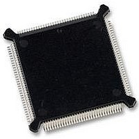
MC68331CEH25 Freescale Semiconductor, MC68331CEH25 Datasheet - Page 92

MC68331CEH25
Manufacturer Part Number
MC68331CEH25
Description
IC MCU 32BIT 25MHZ 132-PQFP
Manufacturer
Freescale Semiconductor
Series
M683xxr
Specifications of MC68331CEH25
Core Processor
CPU32
Core Size
32-Bit
Speed
25MHz
Connectivity
EBI/EMI, SCI, SPI, UART/USART
Peripherals
POR, PWM, WDT
Number Of I /o
18
Program Memory Type
ROMless
Voltage - Supply (vcc/vdd)
4.5 V ~ 5.5 V
Oscillator Type
Internal
Operating Temperature
-40°C ~ 85°C
Package / Case
132-QFP
Controller Family/series
68K
No. Of I/o's
18
Cpu Speed
25MHz
No. Of Timers
1
Embedded Interface Type
QSPI, SCI, UART
No. Of Pwm Channels
2
Digital Ic Case Style
PQFP
Rohs Compliant
Yes
Processor Series
M683xx
Core
CPU32
Data Bus Width
32 bit
Data Ram Size
80 B
Interface Type
QSPI, SCI, UART
Maximum Clock Frequency
25 MHz
Number Of Programmable I/os
18
Number Of Timers
1
Maximum Operating Temperature
+ 85 C
Mounting Style
SMD/SMT
Minimum Operating Temperature
- 40 C
Eeprom Size
-
Ram Size
-
Program Memory Size
-
Data Converters
-
Lead Free Status / Rohs Status
Details
Available stocks
Company
Part Number
Manufacturer
Quantity
Price
Company:
Part Number:
MC68331CEH25
Manufacturer:
PANASONIC
Quantity:
2 000
Company:
Part Number:
MC68331CEH25
Manufacturer:
Freescale Semiconductor
Quantity:
135
Company:
Part Number:
MC68331CEH25
Manufacturer:
Freescale Semiconductor
Quantity:
10 000
- Current page: 92 of 254
- Download datasheet (7Mb)
4
4.8.1 Chip-Select Registers
4-50
transfer size. The chip-select option must not be written until a base address has been
written to a proper base address register. CSBOOT is automatically asserted out of
reset. Alternate functions for chip-select pins are enabled if appropriate data bus pins
are held low at the release of the reset signal (refer to 4.6.3.1 Data Bus Mode Selec-
tion for more information). Figure 4-18 is a functional diagram of a single chip-select
circuit.
Each chip-select pin can have one or more functions. Ship-select pin assignment reg-
isters (CSPAR[0:1]) determine functions of the pins. Pin assignment registers also de-
termine port size (8- or 16-bit) for dynamic bus allocation. A pin data register (PORTC)
latches data for chip-select pins that are used for discrete output.
Blocks of addresses are assigned to each chip-select function. Block sizes of two
Kbytes to one Mbyte can be selected by writing values to the appropriate base address
register (CSBAR[0:10], CSBARBT). Address blocks for separate chip-select functions
can overlap.
Chip select option registers (CSOR[0:10], CSORBT) determine timing of and condi-
tions for assertion of chip-select signals. Eight parameters, including operating mode,
access size, synchronization, and wait state insertion can be specified.
Initialization software usually resides in a peripheral memory device controlled by the
chip-select circuits. A set of special chip-select functions and registers (CSORBT, CS-
BARBT) is provided to support bootstrap operation.
Comprehensive address maps and register diagrams are provided in APPENDIX D
REGISTER SUMMARY.
BUS CONTROL
DSACK
AVEC
INTERNAL
ADDRESS
SIGNALS
Figure 4-18 Chip-Select Circuit Block Diagram
GENERATOR
AVEC
Freescale Semiconductor, Inc.
For More Information On This Product,
BASE ADDRESS REGISTER
ADDRESS COMPARATOR
OPTION REGISTER
OPTION COMPARE
SYSTEM INTEGRATION MODULE
Go to: www.freescale.com
GENERATOR
DSACK
ASSIGNMENT
REGISTER
PIN
CONTROL
TIMING
AND
REGISTER
DATA
PIN
USER’S MANUAL
PIN
CHIP SEL BLOCK
MC68331
Related parts for MC68331CEH25
Image
Part Number
Description
Manufacturer
Datasheet
Request
R
Part Number:
Description:
Mc68331 32 Bit Microcontroller
Manufacturer:
Freescale Semiconductor, Inc
Datasheet:
Part Number:
Description:
Manufacturer:
Freescale Semiconductor, Inc
Datasheet:
Part Number:
Description:
Manufacturer:
Freescale Semiconductor, Inc
Datasheet:
Part Number:
Description:
Manufacturer:
Freescale Semiconductor, Inc
Datasheet:
Part Number:
Description:
Manufacturer:
Freescale Semiconductor, Inc
Datasheet:
Part Number:
Description:
Manufacturer:
Freescale Semiconductor, Inc
Datasheet:
Part Number:
Description:
Manufacturer:
Freescale Semiconductor, Inc
Datasheet:
Part Number:
Description:
Manufacturer:
Freescale Semiconductor, Inc
Datasheet:
Part Number:
Description:
Manufacturer:
Freescale Semiconductor, Inc
Datasheet:
Part Number:
Description:
Manufacturer:
Freescale Semiconductor, Inc
Datasheet:
Part Number:
Description:
Manufacturer:
Freescale Semiconductor, Inc
Datasheet:
Part Number:
Description:
Manufacturer:
Freescale Semiconductor, Inc
Datasheet:
Part Number:
Description:
Manufacturer:
Freescale Semiconductor, Inc
Datasheet:
Part Number:
Description:
Manufacturer:
Freescale Semiconductor, Inc
Datasheet:
Part Number:
Description:
Manufacturer:
Freescale Semiconductor, Inc
Datasheet:


