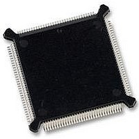
MC68331CEH25 Freescale Semiconductor, MC68331CEH25 Datasheet - Page 130

MC68331CEH25
Manufacturer Part Number
MC68331CEH25
Description
IC MCU 32BIT 25MHZ 132-PQFP
Manufacturer
Freescale Semiconductor
Series
M683xxr
Specifications of MC68331CEH25
Core Processor
CPU32
Core Size
32-Bit
Speed
25MHz
Connectivity
EBI/EMI, SCI, SPI, UART/USART
Peripherals
POR, PWM, WDT
Number Of I /o
18
Program Memory Type
ROMless
Voltage - Supply (vcc/vdd)
4.5 V ~ 5.5 V
Oscillator Type
Internal
Operating Temperature
-40°C ~ 85°C
Package / Case
132-QFP
Controller Family/series
68K
No. Of I/o's
18
Cpu Speed
25MHz
No. Of Timers
1
Embedded Interface Type
QSPI, SCI, UART
No. Of Pwm Channels
2
Digital Ic Case Style
PQFP
Rohs Compliant
Yes
Processor Series
M683xx
Core
CPU32
Data Bus Width
32 bit
Data Ram Size
80 B
Interface Type
QSPI, SCI, UART
Maximum Clock Frequency
25 MHz
Number Of Programmable I/os
18
Number Of Timers
1
Maximum Operating Temperature
+ 85 C
Mounting Style
SMD/SMT
Minimum Operating Temperature
- 40 C
Eeprom Size
-
Ram Size
-
Program Memory Size
-
Data Converters
-
Lead Free Status / Rohs Status
Details
Available stocks
Company
Part Number
Manufacturer
Quantity
Price
Company:
Part Number:
MC68331CEH25
Manufacturer:
PANASONIC
Quantity:
2 000
Company:
Part Number:
MC68331CEH25
Manufacturer:
Freescale Semiconductor
Quantity:
135
Company:
Part Number:
MC68331CEH25
Manufacturer:
Freescale Semiconductor
Quantity:
10 000
- Current page: 130 of 254
- Download datasheet (7Mb)
6
6.2.2 QSM Pin Control Registers
6-4
The QSM uses nine pins. Eight of the pins can be used for serial communication or for
parallel I/O. Clearing a bit in the port QS pin assignment register (PQSPAR) assigns
the corresponding pin to general-purpose I/O; setting a bit assigns the pin to the QSPI.
PQSPAR does not affect operation of the SCI.
The port QS data direction register (DDRQS) determines whether pins are inputs or
outputs. Clearing a bit makes the corresponding pin an input; setting a bit makes the
pin an output. DDRQS affects both QSPI function and I/O function. DDQS1 deter-
mines the direction of the TXD pin only when the SCI transmitter is disabled. When the
SCI transmitter is enabled, the TXD pin is an output. PQSPAR and DDRQS are 8-bit
registers located at the same word address. Table 6-1 is a summary of QSM pin func-
tions.
The port QS data register (PORTQS) latches I/O data. Writes to PORTQS drive pins
defined as outputs. PORTQS reads return data present on the pins when the read is
made. To avoid driving undefined data, first write PORTQS, then configure DDRQS.
1. PQS2 is a digital I/O pin unless the SPI is enabled (SPE in SPCR1 set), in which case it becomes the SPI
2. PQS7 is a digital I/O pin unless the SCI transmitter is enabled (TE in SCCR1 set), in which case it becomes
serial clock SCK.
SCI serial output TXD and DDRQS has no effect.
PCS0/SS
QSM Pin
PCS[3:1]
MISO
MOSI
SCK
TXD
RXD
2
1
Transmit
Receive
Master
Master
Master
Master
Master
Mode
Slave
Slave
Slave
Slave
Slave
Freescale Semiconductor, Inc.
For More Information On This Product,
DDRQS Bit
DDQS[4:6]
DDQS0
DDQS1
DDQS2
DDQS3
DDQS7
Table 6-1 QSM Pin Function
None
QUEUED SERIAL MODULE
Go to: www.freescale.com
State
NA
Bit
0
1
0
1
0
1
0
1
0
1
0
1
0
1
0
1
0
1
0
1
X
Serial Data Output from QSPI
Serial Data Output from QSPI
Assertion Causes Mode Fault
Disables Chip-Select Output
Serial Data Output from SCI
Serial Data Input to QSPI
Serial Data Input to QSPI
Clock Output from QSPI
QSPI Slave Select Input
Serial Data Input to SCI
Disables Clock Output
Disables Data Output
Disables Data Output
Disables Select Input
Disables Clock Input
Clock Input to QSPI
Disables Data Input
Disables Data Input
Chip-Select Output
Chip-Select Output
Pin Function
Inactive
Inactive
USER’S MANUAL
MC68331
Related parts for MC68331CEH25
Image
Part Number
Description
Manufacturer
Datasheet
Request
R
Part Number:
Description:
Mc68331 32 Bit Microcontroller
Manufacturer:
Freescale Semiconductor, Inc
Datasheet:
Part Number:
Description:
Manufacturer:
Freescale Semiconductor, Inc
Datasheet:
Part Number:
Description:
Manufacturer:
Freescale Semiconductor, Inc
Datasheet:
Part Number:
Description:
Manufacturer:
Freescale Semiconductor, Inc
Datasheet:
Part Number:
Description:
Manufacturer:
Freescale Semiconductor, Inc
Datasheet:
Part Number:
Description:
Manufacturer:
Freescale Semiconductor, Inc
Datasheet:
Part Number:
Description:
Manufacturer:
Freescale Semiconductor, Inc
Datasheet:
Part Number:
Description:
Manufacturer:
Freescale Semiconductor, Inc
Datasheet:
Part Number:
Description:
Manufacturer:
Freescale Semiconductor, Inc
Datasheet:
Part Number:
Description:
Manufacturer:
Freescale Semiconductor, Inc
Datasheet:
Part Number:
Description:
Manufacturer:
Freescale Semiconductor, Inc
Datasheet:
Part Number:
Description:
Manufacturer:
Freescale Semiconductor, Inc
Datasheet:
Part Number:
Description:
Manufacturer:
Freescale Semiconductor, Inc
Datasheet:
Part Number:
Description:
Manufacturer:
Freescale Semiconductor, Inc
Datasheet:
Part Number:
Description:
Manufacturer:
Freescale Semiconductor, Inc
Datasheet:


