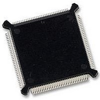
MC68331CEH25 Freescale Semiconductor, MC68331CEH25 Datasheet - Page 241

MC68331CEH25
Manufacturer Part Number
MC68331CEH25
Description
IC MCU 32BIT 25MHZ 132-PQFP
Manufacturer
Freescale Semiconductor
Series
M683xxr
Specifications of MC68331CEH25
Core Processor
CPU32
Core Size
32-Bit
Speed
25MHz
Connectivity
EBI/EMI, SCI, SPI, UART/USART
Peripherals
POR, PWM, WDT
Number Of I /o
18
Program Memory Type
ROMless
Voltage - Supply (vcc/vdd)
4.5 V ~ 5.5 V
Oscillator Type
Internal
Operating Temperature
-40°C ~ 85°C
Package / Case
132-QFP
Controller Family/series
68K
No. Of I/o's
18
Cpu Speed
25MHz
No. Of Timers
1
Embedded Interface Type
QSPI, SCI, UART
No. Of Pwm Channels
2
Digital Ic Case Style
PQFP
Rohs Compliant
Yes
Processor Series
M683xx
Core
CPU32
Data Bus Width
32 bit
Data Ram Size
80 B
Interface Type
QSPI, SCI, UART
Maximum Clock Frequency
25 MHz
Number Of Programmable I/os
18
Number Of Timers
1
Maximum Operating Temperature
+ 85 C
Mounting Style
SMD/SMT
Minimum Operating Temperature
- 40 C
Eeprom Size
-
Ram Size
-
Program Memory Size
-
Data Converters
-
Lead Free Status / Rohs Status
Details
Available stocks
Company
Part Number
Manufacturer
Quantity
Price
Company:
Part Number:
MC68331CEH25
Manufacturer:
PANASONIC
Quantity:
2 000
Company:
Part Number:
MC68331CEH25
Manufacturer:
Freescale Semiconductor
Quantity:
135
Company:
Part Number:
MC68331CEH25
Manufacturer:
Freescale Semiconductor
Quantity:
10 000
- Current page: 241 of 254
- Download datasheet (7Mb)
WOMQ — Wired-OR Mode for QSPI Pins
BITS — Bits Per Transfer
CPOL — Clock Polarity
CPHA — Clock Phase
SPBR — Serial Clock Baud Rate
D.4.11 SPCR1 — QSPI Control Register 1
SPE — QSPI Enable
DSCKL — Delay before SCK
MC68331
USER’S MANUAL
DTL — Length of Delay after Transfer
SPE
15
0
The BITS field determines the number of serial data bits transferred.
QSPI baud rate is selected by writing a value from 2 to 255 into SPBR. Giving BR a
value of zero or one disables SCK (disable state determined by CPOL).
SPCR1 enables the QSPI and specified transfer delays. The CPU32 has read/write
access to SPCR1, but the QSM has read access only to all bits but enable bit SPE.
SPCR1 must be written last during initialization because it contains SPE. Writing a
new value to SPCR1 while the QSPI is enabled disrupts operation.
When the DSCK bit in command RAM is set, this field determines the length of delay
from PCS valid to SCK transition. PCS can be any of the four peripheral chip-select
pins.
When the DT bit in command RAM is set, this field determines the length of delay after
serial transfer.
RESET:
0 = Outputs have normal MOS drivers.
1 = Pins designated for output by DDRQS have open-drain drivers.
0 = The inactive state value of SCK is logic level zero.
1 = The inactive state value of SCK is logic level one.
0 =Data captured on the leading edge of SCK and changed on the following edge
1 =Data is changed on the leading edge of SCK and captured on the following
0 = QSPI is disabled. QSPI pins can be used for general-purpose I/O.
1 = QSPI is enabled. Pins allocated by PQSPAR are controlled by the QSPI.
14
0
of SCK.
edge of SCK.
0
0
Freescale Semiconductor, Inc.
DSCKL
For More Information On This Product,
0
1
Go to: www.freescale.com
REGISTER SUMMARY
0
8
0
7
0
0
0
0
DTL
0
1
$YFFC1A
0
D-33
0
0
D
Related parts for MC68331CEH25
Image
Part Number
Description
Manufacturer
Datasheet
Request
R
Part Number:
Description:
Mc68331 32 Bit Microcontroller
Manufacturer:
Freescale Semiconductor, Inc
Datasheet:
Part Number:
Description:
Manufacturer:
Freescale Semiconductor, Inc
Datasheet:
Part Number:
Description:
Manufacturer:
Freescale Semiconductor, Inc
Datasheet:
Part Number:
Description:
Manufacturer:
Freescale Semiconductor, Inc
Datasheet:
Part Number:
Description:
Manufacturer:
Freescale Semiconductor, Inc
Datasheet:
Part Number:
Description:
Manufacturer:
Freescale Semiconductor, Inc
Datasheet:
Part Number:
Description:
Manufacturer:
Freescale Semiconductor, Inc
Datasheet:
Part Number:
Description:
Manufacturer:
Freescale Semiconductor, Inc
Datasheet:
Part Number:
Description:
Manufacturer:
Freescale Semiconductor, Inc
Datasheet:
Part Number:
Description:
Manufacturer:
Freescale Semiconductor, Inc
Datasheet:
Part Number:
Description:
Manufacturer:
Freescale Semiconductor, Inc
Datasheet:
Part Number:
Description:
Manufacturer:
Freescale Semiconductor, Inc
Datasheet:
Part Number:
Description:
Manufacturer:
Freescale Semiconductor, Inc
Datasheet:
Part Number:
Description:
Manufacturer:
Freescale Semiconductor, Inc
Datasheet:
Part Number:
Description:
Manufacturer:
Freescale Semiconductor, Inc
Datasheet:


