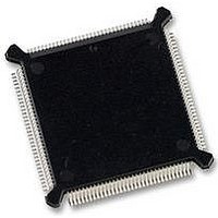
MC68331CEH25 Freescale Semiconductor, MC68331CEH25 Datasheet - Page 238

MC68331CEH25
Manufacturer Part Number
MC68331CEH25
Description
IC MCU 32BIT 25MHZ 132-PQFP
Manufacturer
Freescale Semiconductor
Series
M683xxr
Specifications of MC68331CEH25
Core Processor
CPU32
Core Size
32-Bit
Speed
25MHz
Connectivity
EBI/EMI, SCI, SPI, UART/USART
Peripherals
POR, PWM, WDT
Number Of I /o
18
Program Memory Type
ROMless
Voltage - Supply (vcc/vdd)
4.5 V ~ 5.5 V
Oscillator Type
Internal
Operating Temperature
-40°C ~ 85°C
Package / Case
132-QFP
Controller Family/series
68K
No. Of I/o's
18
Cpu Speed
25MHz
No. Of Timers
1
Embedded Interface Type
QSPI, SCI, UART
No. Of Pwm Channels
2
Digital Ic Case Style
PQFP
Rohs Compliant
Yes
Processor Series
M683xx
Core
CPU32
Data Bus Width
32 bit
Data Ram Size
80 B
Interface Type
QSPI, SCI, UART
Maximum Clock Frequency
25 MHz
Number Of Programmable I/os
18
Number Of Timers
1
Maximum Operating Temperature
+ 85 C
Mounting Style
SMD/SMT
Minimum Operating Temperature
- 40 C
Eeprom Size
-
Ram Size
-
Program Memory Size
-
Data Converters
-
Lead Free Status / Rohs Status
Details
Available stocks
Company
Part Number
Manufacturer
Quantity
Price
Company:
Part Number:
MC68331CEH25
Manufacturer:
PANASONIC
Quantity:
2 000
Company:
Part Number:
MC68331CEH25
Manufacturer:
Freescale Semiconductor
Quantity:
135
Company:
Part Number:
MC68331CEH25
Manufacturer:
Freescale Semiconductor
Quantity:
10 000
- Current page: 238 of 254
- Download datasheet (7Mb)
D
FE — Framing Error
PF — Parity Error
D.4.7 SCDR — SCI Data Register
D.4.8 PORTQS — Port QS Data Register
D.4.9 PQSPAR — PORT QS Pin Assignment Register
D-30
15
15
15
0
0
0
0
SCDR consists of two data registers located at the same address. RDR is a read-only
register that contains data received by the SCI serial interface. Data comes into the
receive serial shifter and is transferred to RDR. TDR is a write-only register that con-
tains data to be transmitted. Data is first written to TDR, then transferred to the transmit
serial shifter, where additional format bits are added before transmission. R[7:0]/T[7:0]
contain either the first eight data bits received when SCDR is read, or the first eight
data bits to be transmitted when SCDR is written. R8/T8 are used when the SCI is con-
figured for 9-bit operation. When the SCI is configured for 8-bit operation, R8/T8 have
no meaning or effect.
PORTQS latches I/O data. Writes drive pins defined as outputs. Reads return data
present on the pins. To avoid driving undefined data, first write a byte to PORTQS,
then configure DDRQS.
Clearing a bit in PQSPAR assigns the corresponding pin to general-purpose I/O; set-
ting a bit assigns the pin to the QSPI. PQSPAR does not affect operation of the SCI.
RESET:
RESET:
0 = No framing error on the received data
1 = Framing error or break occurred on the received data.
0 = No parity error on the received data
1 = Parity error occurred on the received data.
DDRQS — PORT QS Data Direction Register
PQSPA6 PQSPA5 PQSPA4 PQSPA3
14
14
0
0
0
13
13
0
0
0
NOT USED
12
12
0
0
0
Freescale Semiconductor, Inc.
11
11
For More Information On This Product,
0
0
0
10
10
0
0
0
0
Go to: www.freescale.com
REGISTER SUMMARY
PQSPA1 PQSPA0
9
0
0
9
0
R8/T8
U
8
8
8
0
DDQS7
R7/T7
PQS7
7
U
7
0
7
0
RESET:
DDQS6
R6/T6
PQS6
U
6
6
0
6
0
DDQS5
R5/T5
PQS5
U
5
5
0
5
0
DDQS4
R4/T4
PQS4
U
4
4
0
4
0
DDQS3
R3/T3
PQS3
U
3
3
0
3
0
DDQS2
R2/T2
PQS2
USER’S MANUAL
U
2
2
0
2
0
$YFFC0E
DDQS1
R1/T1
PQS1
$YFFC15
$YFFC16
$YFFC17
U
1
1
0
1
0
MC68331
DDQS0
R0/T0
PQS0
0
U
0
0
0
0
Related parts for MC68331CEH25
Image
Part Number
Description
Manufacturer
Datasheet
Request
R
Part Number:
Description:
Mc68331 32 Bit Microcontroller
Manufacturer:
Freescale Semiconductor, Inc
Datasheet:
Part Number:
Description:
Manufacturer:
Freescale Semiconductor, Inc
Datasheet:
Part Number:
Description:
Manufacturer:
Freescale Semiconductor, Inc
Datasheet:
Part Number:
Description:
Manufacturer:
Freescale Semiconductor, Inc
Datasheet:
Part Number:
Description:
Manufacturer:
Freescale Semiconductor, Inc
Datasheet:
Part Number:
Description:
Manufacturer:
Freescale Semiconductor, Inc
Datasheet:
Part Number:
Description:
Manufacturer:
Freescale Semiconductor, Inc
Datasheet:
Part Number:
Description:
Manufacturer:
Freescale Semiconductor, Inc
Datasheet:
Part Number:
Description:
Manufacturer:
Freescale Semiconductor, Inc
Datasheet:
Part Number:
Description:
Manufacturer:
Freescale Semiconductor, Inc
Datasheet:
Part Number:
Description:
Manufacturer:
Freescale Semiconductor, Inc
Datasheet:
Part Number:
Description:
Manufacturer:
Freescale Semiconductor, Inc
Datasheet:
Part Number:
Description:
Manufacturer:
Freescale Semiconductor, Inc
Datasheet:
Part Number:
Description:
Manufacturer:
Freescale Semiconductor, Inc
Datasheet:
Part Number:
Description:
Manufacturer:
Freescale Semiconductor, Inc
Datasheet:


