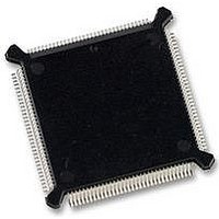
MC68331CEH25 Freescale Semiconductor, MC68331CEH25 Datasheet - Page 230

MC68331CEH25
Manufacturer Part Number
MC68331CEH25
Description
IC MCU 32BIT 25MHZ 132-PQFP
Manufacturer
Freescale Semiconductor
Series
M683xxr
Specifications of MC68331CEH25
Core Processor
CPU32
Core Size
32-Bit
Speed
25MHz
Connectivity
EBI/EMI, SCI, SPI, UART/USART
Peripherals
POR, PWM, WDT
Number Of I /o
18
Program Memory Type
ROMless
Voltage - Supply (vcc/vdd)
4.5 V ~ 5.5 V
Oscillator Type
Internal
Operating Temperature
-40°C ~ 85°C
Package / Case
132-QFP
Controller Family/series
68K
No. Of I/o's
18
Cpu Speed
25MHz
No. Of Timers
1
Embedded Interface Type
QSPI, SCI, UART
No. Of Pwm Channels
2
Digital Ic Case Style
PQFP
Rohs Compliant
Yes
Processor Series
M683xx
Core
CPU32
Data Bus Width
32 bit
Data Ram Size
80 B
Interface Type
QSPI, SCI, UART
Maximum Clock Frequency
25 MHz
Number Of Programmable I/os
18
Number Of Timers
1
Maximum Operating Temperature
+ 85 C
Mounting Style
SMD/SMT
Minimum Operating Temperature
- 40 C
Eeprom Size
-
Ram Size
-
Program Memory Size
-
Data Converters
-
Lead Free Status / Rohs Status
Details
Available stocks
Company
Part Number
Manufacturer
Quantity
Price
Company:
Part Number:
MC68331CEH25
Manufacturer:
PANASONIC
Quantity:
2 000
Company:
Part Number:
MC68331CEH25
Manufacturer:
Freescale Semiconductor
Quantity:
135
Company:
Part Number:
MC68331CEH25
Manufacturer:
Freescale Semiconductor
Quantity:
10 000
- Current page: 230 of 254
- Download datasheet (7Mb)
D
D.3.24 CSPAR1 — Chip Select Pin Assignment Register 1
D-22
15
0
0
RESET:
Contains seven 2-bit fields, CSPA0[6:1] and CSBOOT, that determine the functions of
corresponding chip-select pins. CSPAR0[15:14] are not used. These bits always read
zero; write has no effect. CSPAR0 bit 1 always reads one; writes to CSPAR0 bit 1 have
no effect. The alternate functions can be enabled by data bus mode selection during
reset.
Contains five 2-bit fields (CSPA1[4:0]) that determine the functions of corresponding
chip-select pins. CSPAR1[15:10] are not used. These bits always read zero; write has
no effect. The CSPAR1 pin assignments table shows alternate functions that can be
enabled by data bus mode selection during reset.
14
0
0
Table D-10 CSPAR0 and CSPAR1 Pin Assignment Field Encoding
13
0
0
CSPAR0 Field
CSPAR1 Field
CSPA0[6]
CSPA0[5]
CSPA0[4]
CSPA0[3]
CSPA0[2]
CSPA0[1]
CSBOOT
12
CSPA1[4]
CSPA1[3]
CSPA1[2]
CSPA1[1]
CSPA1[0]
0
0
11
0
0
Freescale Semiconductor, Inc.
*Does not apply to the CSBOOT field
10
Table D-8 CSPAR0 Pin Assignments
Table D-9 CSPAR1 Pin Assignments
0
0
For More Information On This Product,
Bit Field
DATA7
CSPAR0 Signal
CSPAR1 Signal
9
CSPA1[4]
00
01
10
11
CSBOOT
Go to: www.freescale.com
CS10
REGISTER SUMMARY
CS5
CS4
CS3
CS2
CS1
CS0
CS9
CS8
CS7
CS6
8
1
DATA6
7
CSPA1[3]
Chip Select (16-Bit Port)
Chip Select (8-Bit Port)
Alternate Function*
Alternate Signal
Discrete Output*
Alternate Signal
Description
6
1
ADDR23
ADDR22
ADDR21
ADDR20
ADDR19
BGACK
FC2
FC1
FC0
BG
BR
—
DATA5
5
CSPA1[2]
4
1
Discrete Output
Discrete Output
DATA4
ECLK
PC6
PC5
PC4
PC3
3
CSPA1[1]
PC2
PC1
PC0
—
—
—
—
2
1
USER’S MANUAL
DATA3
$YFFA46
1
CSPA1[0]
MC68331
0
1
Related parts for MC68331CEH25
Image
Part Number
Description
Manufacturer
Datasheet
Request
R
Part Number:
Description:
Mc68331 32 Bit Microcontroller
Manufacturer:
Freescale Semiconductor, Inc
Datasheet:
Part Number:
Description:
Manufacturer:
Freescale Semiconductor, Inc
Datasheet:
Part Number:
Description:
Manufacturer:
Freescale Semiconductor, Inc
Datasheet:
Part Number:
Description:
Manufacturer:
Freescale Semiconductor, Inc
Datasheet:
Part Number:
Description:
Manufacturer:
Freescale Semiconductor, Inc
Datasheet:
Part Number:
Description:
Manufacturer:
Freescale Semiconductor, Inc
Datasheet:
Part Number:
Description:
Manufacturer:
Freescale Semiconductor, Inc
Datasheet:
Part Number:
Description:
Manufacturer:
Freescale Semiconductor, Inc
Datasheet:
Part Number:
Description:
Manufacturer:
Freescale Semiconductor, Inc
Datasheet:
Part Number:
Description:
Manufacturer:
Freescale Semiconductor, Inc
Datasheet:
Part Number:
Description:
Manufacturer:
Freescale Semiconductor, Inc
Datasheet:
Part Number:
Description:
Manufacturer:
Freescale Semiconductor, Inc
Datasheet:
Part Number:
Description:
Manufacturer:
Freescale Semiconductor, Inc
Datasheet:
Part Number:
Description:
Manufacturer:
Freescale Semiconductor, Inc
Datasheet:
Part Number:
Description:
Manufacturer:
Freescale Semiconductor, Inc
Datasheet:


