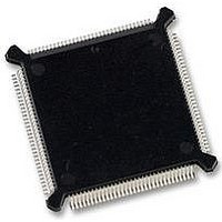
MC68331CEH25 Freescale Semiconductor, MC68331CEH25 Datasheet - Page 134

MC68331CEH25
Manufacturer Part Number
MC68331CEH25
Description
IC MCU 32BIT 25MHZ 132-PQFP
Manufacturer
Freescale Semiconductor
Series
M683xxr
Specifications of MC68331CEH25
Core Processor
CPU32
Core Size
32-Bit
Speed
25MHz
Connectivity
EBI/EMI, SCI, SPI, UART/USART
Peripherals
POR, PWM, WDT
Number Of I /o
18
Program Memory Type
ROMless
Voltage - Supply (vcc/vdd)
4.5 V ~ 5.5 V
Oscillator Type
Internal
Operating Temperature
-40°C ~ 85°C
Package / Case
132-QFP
Controller Family/series
68K
No. Of I/o's
18
Cpu Speed
25MHz
No. Of Timers
1
Embedded Interface Type
QSPI, SCI, UART
No. Of Pwm Channels
2
Digital Ic Case Style
PQFP
Rohs Compliant
Yes
Processor Series
M683xx
Core
CPU32
Data Bus Width
32 bit
Data Ram Size
80 B
Interface Type
QSPI, SCI, UART
Maximum Clock Frequency
25 MHz
Number Of Programmable I/os
18
Number Of Timers
1
Maximum Operating Temperature
+ 85 C
Mounting Style
SMD/SMT
Minimum Operating Temperature
- 40 C
Eeprom Size
-
Ram Size
-
Program Memory Size
-
Data Converters
-
Lead Free Status / Rohs Status
Details
Available stocks
Company
Part Number
Manufacturer
Quantity
Price
Company:
Part Number:
MC68331CEH25
Manufacturer:
PANASONIC
Quantity:
2 000
Company:
Part Number:
MC68331CEH25
Manufacturer:
Freescale Semiconductor
Quantity:
135
Company:
Part Number:
MC68331CEH25
Manufacturer:
Freescale Semiconductor
Quantity:
10 000
- Current page: 134 of 254
- Download datasheet (7Mb)
6
6.3.2.1 Receive RAM
6.3.2.2 Transmit RAM
6.3.2.3 Command RAM
6.3.3 QSPI Pins
6-8
Data received by the QSPI is stored in this segment. The CPU reads this segment to
retrieve data from the QSPI. Data stored in receive RAM is right-justified. Unused bits
in a receive queue entry are set to zero by the QSPI upon completion of the individual
queue entry. The CPU can access the data using byte, word, or long-word addressing.
The CPTQP value in SPSR shows which queue entries have been executed. The CPU
uses this information to determine which locations in receive RAM contain valid data
before reading them.
Data that is to be transmitted by the QSPI is stored in this segment. The CPU normally
writes one word of data into this segment for each queue command to be executed.
Information to be transmitted must be written to transmit RAM in a right-justified for-
mat. The QSPI cannot modify information in the transmit RAM. The QSPI copies the
information to its data serializer for transmission. Information remains in transmit RAM
until overwritten.
Command RAM is used by the QSPI in master mode. The CPU writes one byte of con-
trol information to this segment for each QSPI command to be executed. The QSPI
cannot modify information in command RAM.
Command RAM consists of 16 bytes. Each byte is divided into two fields. The periph-
eral chip-select field enables peripherals for transfer. The command control field pro-
vides transfer options.
A maximum of 16 commands can be in the queue. Queue execution by the QSPI pro-
ceeds from the address in NEWQP through the address in ENDQP (both of these
fields are in SPCR2).
The QSPI uses seven pins. These pins can be configured for general-purpose I/O
when not needed for QSPI application. When used for QSPI functions, the MOSI, MI-
SO, and SS pins should have pull-up resistors.
Table 6-2 shows QSPI input and output pins and their functions.
Freescale Semiconductor, Inc.
For More Information On This Product,
QUEUED SERIAL MODULE
Go to: www.freescale.com
USER’S MANUAL
MC68331
Related parts for MC68331CEH25
Image
Part Number
Description
Manufacturer
Datasheet
Request
R
Part Number:
Description:
Mc68331 32 Bit Microcontroller
Manufacturer:
Freescale Semiconductor, Inc
Datasheet:
Part Number:
Description:
Manufacturer:
Freescale Semiconductor, Inc
Datasheet:
Part Number:
Description:
Manufacturer:
Freescale Semiconductor, Inc
Datasheet:
Part Number:
Description:
Manufacturer:
Freescale Semiconductor, Inc
Datasheet:
Part Number:
Description:
Manufacturer:
Freescale Semiconductor, Inc
Datasheet:
Part Number:
Description:
Manufacturer:
Freescale Semiconductor, Inc
Datasheet:
Part Number:
Description:
Manufacturer:
Freescale Semiconductor, Inc
Datasheet:
Part Number:
Description:
Manufacturer:
Freescale Semiconductor, Inc
Datasheet:
Part Number:
Description:
Manufacturer:
Freescale Semiconductor, Inc
Datasheet:
Part Number:
Description:
Manufacturer:
Freescale Semiconductor, Inc
Datasheet:
Part Number:
Description:
Manufacturer:
Freescale Semiconductor, Inc
Datasheet:
Part Number:
Description:
Manufacturer:
Freescale Semiconductor, Inc
Datasheet:
Part Number:
Description:
Manufacturer:
Freescale Semiconductor, Inc
Datasheet:
Part Number:
Description:
Manufacturer:
Freescale Semiconductor, Inc
Datasheet:
Part Number:
Description:
Manufacturer:
Freescale Semiconductor, Inc
Datasheet:


