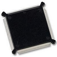
MC68331CEH25 Freescale Semiconductor, MC68331CEH25 Datasheet - Page 187

MC68331CEH25
Manufacturer Part Number
MC68331CEH25
Description
IC MCU 32BIT 25MHZ 132-PQFP
Manufacturer
Freescale Semiconductor
Series
M683xxr
Specifications of MC68331CEH25
Core Processor
CPU32
Core Size
32-Bit
Speed
25MHz
Connectivity
EBI/EMI, SCI, SPI, UART/USART
Peripherals
POR, PWM, WDT
Number Of I /o
18
Program Memory Type
ROMless
Voltage - Supply (vcc/vdd)
4.5 V ~ 5.5 V
Oscillator Type
Internal
Operating Temperature
-40°C ~ 85°C
Package / Case
132-QFP
Controller Family/series
68K
No. Of I/o's
18
Cpu Speed
25MHz
No. Of Timers
1
Embedded Interface Type
QSPI, SCI, UART
No. Of Pwm Channels
2
Digital Ic Case Style
PQFP
Rohs Compliant
Yes
Processor Series
M683xx
Core
CPU32
Data Bus Width
32 bit
Data Ram Size
80 B
Interface Type
QSPI, SCI, UART
Maximum Clock Frequency
25 MHz
Number Of Programmable I/os
18
Number Of Timers
1
Maximum Operating Temperature
+ 85 C
Mounting Style
SMD/SMT
Minimum Operating Temperature
- 40 C
Eeprom Size
-
Ram Size
-
Program Memory Size
-
Data Converters
-
Lead Free Status / Rohs Status
Details
Available stocks
Company
Part Number
Manufacturer
Quantity
Price
Company:
Part Number:
MC68331CEH25
Manufacturer:
PANASONIC
Quantity:
2 000
Company:
Part Number:
MC68331CEH25
Manufacturer:
Freescale Semiconductor
Quantity:
135
Company:
Part Number:
MC68331CEH25
Manufacturer:
Freescale Semiconductor
Quantity:
10 000
MC68331
USER’S MANUAL
10. To ensure coherency during every operand transfer, BG will not be asserted in response to BR until after all
11. In the absence of DSACK[1:0], BERR is an asynchronous input using the asynchronous setup time (specifica-
12. After external RESET negation is detected, a short transition period (approximately 2 t
13. External assertion of the RESET input can overlap internally-generated resets. To insure that an external reset
14. External logic must pull RESET high during this period in order for normal MCU operation to begin.
15. Address access time = (2.5 + WS) t
Notes for Tables A–6 and A–6a:
1. All AC timing is shown with respect to 20% V
2. Minimum system clock frequency is four times the crystal frequency, subject to specified limits.
3. When an external clock is used, minimum high and low times are based on a 50% duty cycle. The minimum
4. Parameters for an external clock signal applied while the internal PLL is disabled (MODCLK pin held low during
5. Specification 9A is the worst-case skew between AS and DS or CS. The amount of skew depends on the relative
6. If multiple chip selects are used, CS width negated (specification 15) applies to the time from the negation of a
7. Hold times are specified with respect to DS or CS on asynchronous reads and with respect to CLKOUT on fast
8. Maximum value is equal to (t
9. If the asynchronous setup time (specification 47A) requirements are satisfied, the DSACK[1:0] low to data setup
cycles of the current operand transfer are complete and RMC is negated.
tion 47A).
drives RESET low for 512 t
is recognized in all cases, RESET must be asserted for at least 590 CLKOUT cycles.
Chip select access time = (2 + WS) t
Where: WS = number of wait states. When fast termination is used (2 clock bus) WS = –1.
allowable t
tween external clock input duty cycle and minimum t
reset). Does not pertain to an external VCO reference applied while the PLL is enabled (MODCLK pin held high
during reset). When the PLL is enabled, the clock synthesizer detects successive transitions of the reference
signal. If transitions occur within the correct clock period, rise/fall times and duty cycle are not critical.
loading of these signals. When loads are kept within specified limits, skew will not cause AS and DS to fall out-
side the limits shown in specification 9.
heavily loaded chip select to the assertion of a lightly loaded chip select. The CS width negated specification
between multiple chip selects does not apply to chip selects being used for synchronous ECLK cycles.
cycle reads. The user is free to use either hold time.
time (specification 31) and DSACK[1:0] low to BERR low setup time (specification 48) can be ignored. The data
must only satisfy the data-in to clock low setup time (specification 27) for the following clock cycle. BERR must
satisfy only the late BERR low to clock low setup time (specification 27A) for the following clock cycle.
Minimum t
Xcyc
period is reduced when the duty cycle of the external clock signal varies. The relationship be-
Xcyc
Freescale Semiconductor, Inc.
period = minimum t
For More Information On This Product,
cyc
cyc
.
ELECTRICAL CHARACTERISTICS
/ 2) + 25 ns.
cyc
Go to: www.freescale.com
cyc
– t
– t
CHAV
CLSA
XCHL
DD
– t
– t
and 70% V
DICL
DICL
/ (50% – external clock input duty cycle tolerance).
Xcyc
is expressed:
DD
levels unless otherwise noted.
cyc
) elapses, then the SIM
A-11
A


