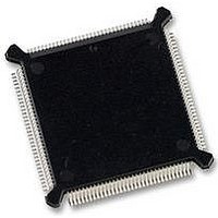
MC68331CEH25 Freescale Semiconductor, MC68331CEH25 Datasheet - Page 80

MC68331CEH25
Manufacturer Part Number
MC68331CEH25
Description
IC MCU 32BIT 25MHZ 132-PQFP
Manufacturer
Freescale Semiconductor
Series
M683xxr
Specifications of MC68331CEH25
Core Processor
CPU32
Core Size
32-Bit
Speed
25MHz
Connectivity
EBI/EMI, SCI, SPI, UART/USART
Peripherals
POR, PWM, WDT
Number Of I /o
18
Program Memory Type
ROMless
Voltage - Supply (vcc/vdd)
4.5 V ~ 5.5 V
Oscillator Type
Internal
Operating Temperature
-40°C ~ 85°C
Package / Case
132-QFP
Controller Family/series
68K
No. Of I/o's
18
Cpu Speed
25MHz
No. Of Timers
1
Embedded Interface Type
QSPI, SCI, UART
No. Of Pwm Channels
2
Digital Ic Case Style
PQFP
Rohs Compliant
Yes
Processor Series
M683xx
Core
CPU32
Data Bus Width
32 bit
Data Ram Size
80 B
Interface Type
QSPI, SCI, UART
Maximum Clock Frequency
25 MHz
Number Of Programmable I/os
18
Number Of Timers
1
Maximum Operating Temperature
+ 85 C
Mounting Style
SMD/SMT
Minimum Operating Temperature
- 40 C
Eeprom Size
-
Ram Size
-
Program Memory Size
-
Data Converters
-
Lead Free Status / Rohs Status
Details
Available stocks
Company
Part Number
Manufacturer
Quantity
Price
Company:
Part Number:
MC68331CEH25
Manufacturer:
PANASONIC
Quantity:
2 000
Company:
Part Number:
MC68331CEH25
Manufacturer:
Freescale Semiconductor
Quantity:
135
Company:
Part Number:
MC68331CEH25
Manufacturer:
Freescale Semiconductor
Quantity:
10 000
- Current page: 80 of 254
- Download datasheet (7Mb)
4
4.6.3.1 Data Bus Mode Selection
4-38
All data lines have weak internal pull-up drivers. When pins are held high by the inter-
nal drivers, the MCU uses a default operating configuration. However, specific lines
can be held low externally to achieve an alternate configuration.
Use an active device to hold data bus lines low. Data bus configuration logic must re-
lease the bus before the first bus cycle after reset to prevent conflict with external
memory devices. The first bus cycle occurs ten CLKOUT cycles after RESET is re-
leased. If external mode selection logic causes a conflict of this type, an isolation re-
sistor on the driven lines may be required. Figure 4-15 shows a recommended method
for conditioning the mode select signals.
Mode Select Pin
MODCLK
External bus loading can overcome the weak internal pull-up drivers
on data bus lines, and hold pins low during reset.
DATA11
DATA0
DATA1
DATA2
DATA3
DATA4
DATA5
DATA6
DATA7
DATA8
DATA9
BKPT
Freescale Semiconductor, Inc.
For More Information On This Product,
Table 4-16 Reset Mode Selection
SYSTEM INTEGRATION MODULE
Go to: www.freescale.com
Background Mode Disabled
VCO = System Clock
Test Mode Disabled
Default Function
CSBOOT 16-Bit
(Pin Left High)
AVEC, DS, AS,
DSACK[1:0],
MODCLK
CS[10:6]
IRQ[7:1]
CS[7:6]
CS[8:6]
CS[9:6]
SIZE
CS0
CS1
CS2
CS3
CS4
CS5
CS6
NOTE
Background Mode Enabled
EXTAL = System Clock
Alternate Function
Test Mode Enabled
(Pin Pulled Low)
CSBOOT 8-Bit
ADDR[20:19]
ADDR[21:19]
ADDR[22:19]
ADDR[23:19]
ADDR19
BGACK
PORTE
PORTF
FC0
FC1
FC2
BR
BG
USER’S MANUAL
MC68331
Related parts for MC68331CEH25
Image
Part Number
Description
Manufacturer
Datasheet
Request
R
Part Number:
Description:
Mc68331 32 Bit Microcontroller
Manufacturer:
Freescale Semiconductor, Inc
Datasheet:
Part Number:
Description:
Manufacturer:
Freescale Semiconductor, Inc
Datasheet:
Part Number:
Description:
Manufacturer:
Freescale Semiconductor, Inc
Datasheet:
Part Number:
Description:
Manufacturer:
Freescale Semiconductor, Inc
Datasheet:
Part Number:
Description:
Manufacturer:
Freescale Semiconductor, Inc
Datasheet:
Part Number:
Description:
Manufacturer:
Freescale Semiconductor, Inc
Datasheet:
Part Number:
Description:
Manufacturer:
Freescale Semiconductor, Inc
Datasheet:
Part Number:
Description:
Manufacturer:
Freescale Semiconductor, Inc
Datasheet:
Part Number:
Description:
Manufacturer:
Freescale Semiconductor, Inc
Datasheet:
Part Number:
Description:
Manufacturer:
Freescale Semiconductor, Inc
Datasheet:
Part Number:
Description:
Manufacturer:
Freescale Semiconductor, Inc
Datasheet:
Part Number:
Description:
Manufacturer:
Freescale Semiconductor, Inc
Datasheet:
Part Number:
Description:
Manufacturer:
Freescale Semiconductor, Inc
Datasheet:
Part Number:
Description:
Manufacturer:
Freescale Semiconductor, Inc
Datasheet:
Part Number:
Description:
Manufacturer:
Freescale Semiconductor, Inc
Datasheet:


