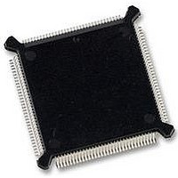
MC68331CEH25 Freescale Semiconductor, MC68331CEH25 Datasheet - Page 144

MC68331CEH25
Manufacturer Part Number
MC68331CEH25
Description
IC MCU 32BIT 25MHZ 132-PQFP
Manufacturer
Freescale Semiconductor
Series
M683xxr
Specifications of MC68331CEH25
Core Processor
CPU32
Core Size
32-Bit
Speed
25MHz
Connectivity
EBI/EMI, SCI, SPI, UART/USART
Peripherals
POR, PWM, WDT
Number Of I /o
18
Program Memory Type
ROMless
Voltage - Supply (vcc/vdd)
4.5 V ~ 5.5 V
Oscillator Type
Internal
Operating Temperature
-40°C ~ 85°C
Package / Case
132-QFP
Controller Family/series
68K
No. Of I/o's
18
Cpu Speed
25MHz
No. Of Timers
1
Embedded Interface Type
QSPI, SCI, UART
No. Of Pwm Channels
2
Digital Ic Case Style
PQFP
Rohs Compliant
Yes
Processor Series
M683xx
Core
CPU32
Data Bus Width
32 bit
Data Ram Size
80 B
Interface Type
QSPI, SCI, UART
Maximum Clock Frequency
25 MHz
Number Of Programmable I/os
18
Number Of Timers
1
Maximum Operating Temperature
+ 85 C
Mounting Style
SMD/SMT
Minimum Operating Temperature
- 40 C
Eeprom Size
-
Ram Size
-
Program Memory Size
-
Data Converters
-
Lead Free Status / Rohs Status
Details
Available stocks
Company
Part Number
Manufacturer
Quantity
Price
Company:
Part Number:
MC68331CEH25
Manufacturer:
PANASONIC
Quantity:
2 000
Company:
Part Number:
MC68331CEH25
Manufacturer:
Freescale Semiconductor
Quantity:
135
Company:
Part Number:
MC68331CEH25
Manufacturer:
Freescale Semiconductor
Quantity:
10 000
- Current page: 144 of 254
- Download datasheet (7Mb)
6
6-18
or
Giving SPBR a value of zero or one disables the baud rate generator. SCK is disabled
and assumes its inactive state value.
The DSCK field in command RAM determines the delay period from chip-select asser-
tion until the leading edge of the serial clock. The DSCKL field in SPCR1 determines
the period of delay before the assertion of SCK. The following expression determines
the actual delay before SCK:
where DSCKL equals {1, 2, 3,..., 127}.
When DSCK equals zero, DSCKL is not used. Instead, the PCS valid-to-SCK transi-
tion is one-half the DSCK period.
There are two transfer length options. The user can choose a default value of eight
bits, or a programmed value of eight to sixteen bits, inclusive. The programmed value
must be written into the BITS field in SPCR0. The BITSE field in command RAM de-
termines whether the default value (BITSE = 0) or the BITS value (BITSE = 1) is used.
Table 6-3 shows BITS field encoding.
Delay after transfer can be used to provide a peripheral deselect interval. A delay can
also be inserted between consecutive transfers to allow serial A/D converters to com-
plete conversion. There are two transfer delay options. The user can choose to delay
a standard period after serial transfer is complete or can specify a delay period. Writing
a value to the DTL field in SPCR1 specifies a delay period. The DT bit in command
RAM determines whether the standard delay period (DT = 0) or the specified delay pe-
SPBR
PCS to SCK Delay
=
--------------------------------------------------------------------------------------- -
2 SCK
System Clock
Freescale Semiconductor, Inc.
=
For More Information On This Product,
----------------------------------------------------------------- -
System Clock Frequency
Baud Rate Desired
BITS
0000
0001
0010
0011
0100
0101
0110
0111
1000
1001
1010
1011
1100
1101
1110
1111
Table 6-3 BITS Encoding
QUEUED SERIAL MODULE
Go to: www.freescale.com
DSCKL
Bits per Transfer
Reserved
Reserved
Reserved
Reserved
Reserved
Reserved
Reserved
16
10
11
12
13
14
15
8
9
USER’S MANUAL
MC68331
Related parts for MC68331CEH25
Image
Part Number
Description
Manufacturer
Datasheet
Request
R
Part Number:
Description:
Mc68331 32 Bit Microcontroller
Manufacturer:
Freescale Semiconductor, Inc
Datasheet:
Part Number:
Description:
Manufacturer:
Freescale Semiconductor, Inc
Datasheet:
Part Number:
Description:
Manufacturer:
Freescale Semiconductor, Inc
Datasheet:
Part Number:
Description:
Manufacturer:
Freescale Semiconductor, Inc
Datasheet:
Part Number:
Description:
Manufacturer:
Freescale Semiconductor, Inc
Datasheet:
Part Number:
Description:
Manufacturer:
Freescale Semiconductor, Inc
Datasheet:
Part Number:
Description:
Manufacturer:
Freescale Semiconductor, Inc
Datasheet:
Part Number:
Description:
Manufacturer:
Freescale Semiconductor, Inc
Datasheet:
Part Number:
Description:
Manufacturer:
Freescale Semiconductor, Inc
Datasheet:
Part Number:
Description:
Manufacturer:
Freescale Semiconductor, Inc
Datasheet:
Part Number:
Description:
Manufacturer:
Freescale Semiconductor, Inc
Datasheet:
Part Number:
Description:
Manufacturer:
Freescale Semiconductor, Inc
Datasheet:
Part Number:
Description:
Manufacturer:
Freescale Semiconductor, Inc
Datasheet:
Part Number:
Description:
Manufacturer:
Freescale Semiconductor, Inc
Datasheet:
Part Number:
Description:
Manufacturer:
Freescale Semiconductor, Inc
Datasheet:


