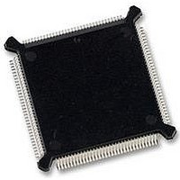
MC68331CEH25 Freescale Semiconductor, MC68331CEH25 Datasheet - Page 200

MC68331CEH25
Manufacturer Part Number
MC68331CEH25
Description
IC MCU 32BIT 25MHZ 132-PQFP
Manufacturer
Freescale Semiconductor
Series
M683xxr
Specifications of MC68331CEH25
Core Processor
CPU32
Core Size
32-Bit
Speed
25MHz
Connectivity
EBI/EMI, SCI, SPI, UART/USART
Peripherals
POR, PWM, WDT
Number Of I /o
18
Program Memory Type
ROMless
Voltage - Supply (vcc/vdd)
4.5 V ~ 5.5 V
Oscillator Type
Internal
Operating Temperature
-40°C ~ 85°C
Package / Case
132-QFP
Controller Family/series
68K
No. Of I/o's
18
Cpu Speed
25MHz
No. Of Timers
1
Embedded Interface Type
QSPI, SCI, UART
No. Of Pwm Channels
2
Digital Ic Case Style
PQFP
Rohs Compliant
Yes
Processor Series
M683xx
Core
CPU32
Data Bus Width
32 bit
Data Ram Size
80 B
Interface Type
QSPI, SCI, UART
Maximum Clock Frequency
25 MHz
Number Of Programmable I/os
18
Number Of Timers
1
Maximum Operating Temperature
+ 85 C
Mounting Style
SMD/SMT
Minimum Operating Temperature
- 40 C
Eeprom Size
-
Ram Size
-
Program Memory Size
-
Data Converters
-
Lead Free Status / Rohs Status
Details
Available stocks
Company
Part Number
Manufacturer
Quantity
Price
Company:
Part Number:
MC68331CEH25
Manufacturer:
PANASONIC
Quantity:
2 000
Company:
Part Number:
MC68331CEH25
Manufacturer:
Freescale Semiconductor
Quantity:
135
Company:
Part Number:
MC68331CEH25
Manufacturer:
Freescale Semiconductor
Quantity:
10 000
- Current page: 200 of 254
- Download datasheet (7Mb)
A
Notes:
1 All AC timing is shown with respect to 20% V
2. In formula, n = External SCK rise + External SCK fall time
3. Data can be recognized properly with longer transition times as long as MOSI/MISO signals from external sources
A-24
Num
10
11
12
13
are at valid V
point voltages of the data and clock signals can differ, which can corrupt data if slower transition times are used.
1
2
3
4
5
6
7
8
9
Operating Frequency
Cycle Time
Enable Lead Time
Enable Lag Time
Clock (SCK) High or Low Time
Sequential Transfer Delay
Data Setup Time (Inputs)
Data Hold Time (Inputs)
Slave Access Time
Slave MISO Disable Time
Data Valid (after SCK Edge)
Data Hold Time (Outputs)
Rise Time
Fall Time
Master
Slave
Master
Slave
Master
Slave
Master
Slave
Master
Slave
Master
Slave (Does Not Require Deselect)
Master
Slave
Master
Slave
Master
Slave
Master
Slave
Input
Output
Input
Output
OH
3
3
2
/V
(V
OL
DD
prior to SCK transitioning between valid V
Function
= 5.0 V
Freescale Semiconductor, Inc.
dc
For More Information On This Product,
10%, V
ELECTRICAL CHARACTERISTICS
Table A-9 QSPI Timing
SS
Go to: www.freescale.com
= 0 Vdc, T
DD
and 70% V
Symbol
t
t
qcyc
t
t
f
lead
t
t
t
t
t
t
t
lag
t
dis
t
op
sw
t
ho
t
su
td
hi
ro
fo
a
ri
v
fi
A
= T
L
DD
to T
2 t
2 t
levels unless otherwise noted.
OL
cyc
H
Min
cyc
DC
DC
17
13
30
20
20
—
—
—
—
—
—
—
—
—
, 200 pF load on all QSPI pins)
4
4
2
2
2
0
0
0
and V
– 60
– n
OH
. Due to process variation, logic decision
255 t
8192
Max
510
128
1/4
1/4
1/2
—
—
—
—
—
—
—
—
—
50
50
—
—
30
30
1
2
2
2
cyc
System Clock Frequency
System Clock Frequency
USER’S MANUAL
SCK
Unit
t
t
t
t
t
t
t
t
t
ns
ns
ns
ns
ns
ns
ns
ns
ns
ns
ns
ns
cyc
cyc
cyc
cyc
cyc
cyc
cyc
cyc
cyc
s
s
MC68331
Related parts for MC68331CEH25
Image
Part Number
Description
Manufacturer
Datasheet
Request
R
Part Number:
Description:
Mc68331 32 Bit Microcontroller
Manufacturer:
Freescale Semiconductor, Inc
Datasheet:
Part Number:
Description:
Manufacturer:
Freescale Semiconductor, Inc
Datasheet:
Part Number:
Description:
Manufacturer:
Freescale Semiconductor, Inc
Datasheet:
Part Number:
Description:
Manufacturer:
Freescale Semiconductor, Inc
Datasheet:
Part Number:
Description:
Manufacturer:
Freescale Semiconductor, Inc
Datasheet:
Part Number:
Description:
Manufacturer:
Freescale Semiconductor, Inc
Datasheet:
Part Number:
Description:
Manufacturer:
Freescale Semiconductor, Inc
Datasheet:
Part Number:
Description:
Manufacturer:
Freescale Semiconductor, Inc
Datasheet:
Part Number:
Description:
Manufacturer:
Freescale Semiconductor, Inc
Datasheet:
Part Number:
Description:
Manufacturer:
Freescale Semiconductor, Inc
Datasheet:
Part Number:
Description:
Manufacturer:
Freescale Semiconductor, Inc
Datasheet:
Part Number:
Description:
Manufacturer:
Freescale Semiconductor, Inc
Datasheet:
Part Number:
Description:
Manufacturer:
Freescale Semiconductor, Inc
Datasheet:
Part Number:
Description:
Manufacturer:
Freescale Semiconductor, Inc
Datasheet:
Part Number:
Description:
Manufacturer:
Freescale Semiconductor, Inc
Datasheet:


