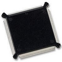
MC68331CEH25 Freescale Semiconductor, MC68331CEH25 Datasheet - Page 155

MC68331CEH25
Manufacturer Part Number
MC68331CEH25
Description
IC MCU 32BIT 25MHZ 132-PQFP
Manufacturer
Freescale Semiconductor
Series
M683xxr
Specifications of MC68331CEH25
Core Processor
CPU32
Core Size
32-Bit
Speed
25MHz
Connectivity
EBI/EMI, SCI, SPI, UART/USART
Peripherals
POR, PWM, WDT
Number Of I /o
18
Program Memory Type
ROMless
Voltage - Supply (vcc/vdd)
4.5 V ~ 5.5 V
Oscillator Type
Internal
Operating Temperature
-40°C ~ 85°C
Package / Case
132-QFP
Controller Family/series
68K
No. Of I/o's
18
Cpu Speed
25MHz
No. Of Timers
1
Embedded Interface Type
QSPI, SCI, UART
No. Of Pwm Channels
2
Digital Ic Case Style
PQFP
Rohs Compliant
Yes
Processor Series
M683xx
Core
CPU32
Data Bus Width
32 bit
Data Ram Size
80 B
Interface Type
QSPI, SCI, UART
Maximum Clock Frequency
25 MHz
Number Of Programmable I/os
18
Number Of Timers
1
Maximum Operating Temperature
+ 85 C
Mounting Style
SMD/SMT
Minimum Operating Temperature
- 40 C
Eeprom Size
-
Ram Size
-
Program Memory Size
-
Data Converters
-
Lead Free Status / Rohs Status
Details
Available stocks
Company
Part Number
Manufacturer
Quantity
Price
Company:
Part Number:
MC68331CEH25
Manufacturer:
PANASONIC
Quantity:
2 000
Company:
Part Number:
MC68331CEH25
Manufacturer:
Freescale Semiconductor
Quantity:
135
Company:
Part Number:
MC68331CEH25
Manufacturer:
Freescale Semiconductor
Quantity:
10 000
6.4.3.6 Receiver Operation
6.4.3.7 Idle-Line Detection
MC68331
USER’S MANUAL
The receiver enable (RE) bit in SCCR1 enables (RE = 1) and disables (RE = 0) the
transmitter. The receiver contains a receive serial shifter and a parallel receive data
register (RDR) located in the SCI data register (SCDR). The serial shifter cannot be
directly accessed by the CPU. The receiver is double-buffered, allowing data to be
held in RDR while other data is shifted in.
Receiver bit processor logic drives a state machine that determines the logic level for
each bit-time. This state machine controls when the bit processor logic is to sample
the RXD pin and also controls when data is to be passed to the receive serial shifter.
A receive time (RT) clock is used to control sampling and synchronization. Data is
shifted into the receive serial shifter according to the most recent synchronization of
the RT clock with the incoming data stream. From this point on, data movement is syn-
chronized with the MCU system clock. Operation of the receiver state machine is de-
tailed in the QSM Reference Manual (QSMRM/AD).
The number of bits shifted in by the receiver depends on the serial format. However,
all frames must end with at least one stop bit. When the stop bit is received, the frame
is considered to be complete, and the received data in the serial shifter is transferred
to the RDR. The receiver data register flag (RDRF) is set when the data is transferred.
Noise errors, parity errors, and framing errors can be detected while a data stream is
being received. Although error conditions are detected as bits are received, the noise
flag (NF), the parity flag (PF), and the framing error (FE) flag in SCSR are not set until
data is transferred from the serial shifter to RDR.
RDRF must be cleared before the next transfer from the shifter can take place. If
RDRF is set when the shifter is full, transfers are inhibited and the overrun error (OR)
flag in the SCSR is set. OR indicates that the CPU needs to service RDR faster. When
OR is set, the data in RDR is preserved, but the data in the serial shifter is lost. Be-
cause framing, noise, and parity errors are detected while data is in the serial shifter,
FE, NF, and PF cannot occur at the same time as OR.
When the CPU reads the SCSR and the SCDR in sequence, it acquires status and
data, and also clears the status flags. Reading the SCSR acquires status and arms
the clearing mechanism. Reading the SCDR acquires data and clears the SCSR.
When RIE in SCCR1 is set, an interrupt request is generated whenever RDRF is set.
Because receiver status flags are set at the same time as RDRF, they do not have
separate interrupt enables.
During a typical serial transmission, frames are transmitted isochronously and no idle
time occurs between frames. Even when all the data bits in a frame are logic ones, the
start bit provides one logic zero bit-time during the frame. An idle line is a sequence of
contiguous ones equal to the current frame size. Frame size is determined by the state
of the M bit in SCCR1.
Freescale Semiconductor, Inc.
For More Information On This Product,
QUEUED SERIAL MODULE
Go to: www.freescale.com
6-29
6


