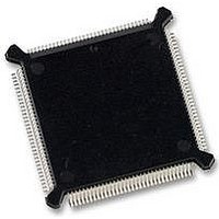
MC68331CEH25 Freescale Semiconductor, MC68331CEH25 Datasheet - Page 123

MC68331CEH25
Manufacturer Part Number
MC68331CEH25
Description
IC MCU 32BIT 25MHZ 132-PQFP
Manufacturer
Freescale Semiconductor
Series
M683xxr
Specifications of MC68331CEH25
Core Processor
CPU32
Core Size
32-Bit
Speed
25MHz
Connectivity
EBI/EMI, SCI, SPI, UART/USART
Peripherals
POR, PWM, WDT
Number Of I /o
18
Program Memory Type
ROMless
Voltage - Supply (vcc/vdd)
4.5 V ~ 5.5 V
Oscillator Type
Internal
Operating Temperature
-40°C ~ 85°C
Package / Case
132-QFP
Controller Family/series
68K
No. Of I/o's
18
Cpu Speed
25MHz
No. Of Timers
1
Embedded Interface Type
QSPI, SCI, UART
No. Of Pwm Channels
2
Digital Ic Case Style
PQFP
Rohs Compliant
Yes
Processor Series
M683xx
Core
CPU32
Data Bus Width
32 bit
Data Ram Size
80 B
Interface Type
QSPI, SCI, UART
Maximum Clock Frequency
25 MHz
Number Of Programmable I/os
18
Number Of Timers
1
Maximum Operating Temperature
+ 85 C
Mounting Style
SMD/SMT
Minimum Operating Temperature
- 40 C
Eeprom Size
-
Ram Size
-
Program Memory Size
-
Data Converters
-
Lead Free Status / Rohs Status
Details
Available stocks
Company
Part Number
Manufacturer
Quantity
Price
Company:
Part Number:
MC68331CEH25
Manufacturer:
PANASONIC
Quantity:
2 000
Company:
Part Number:
MC68331CEH25
Manufacturer:
Freescale Semiconductor
Quantity:
135
Company:
Part Number:
MC68331CEH25
Manufacturer:
Freescale Semiconductor
Quantity:
10 000
- Current page: 123 of 254
- Download datasheet (7Mb)
MC68331
USER’S MANUAL
MICROSEQUENCER
The serial interface uses a full-duplex synchronous protocol similar to the serial pe-
ripheral interface (SPI) protocol. The development system serves as the master of the
serial link since it is responsible for the generation of DSCLK. If DSCLK is derived from
the CPU32 system clock, development system serial logic is unhindered by the oper-
ating frequency of the target processor. Operable frequency range of the serial clock
is from DC to one-half the processor system clock frequency.
The serial interface operates in full-duplex mode —data is transmitted and received
simultaneously by both master and slave devices. In general, data transitions occur on
the falling edge of DSCLK and are stable by the following rising edge of DSCLK. Data
is transmitted MSB first, and is latched on the rising edge of DSCLK.
The serial data word is 17 bits wide — 16 data bits and a status/control bit. Bit 16 in-
dicates the status of CPU-generated messages as shown in Table 5-6.
SYNCHRONIZE
EXECUTION
CPU
STATUS
UNIT
Figure 5-9 Debug Serial I/O Block Diagram
Freescale Semiconductor, Inc.
For More Information On This Product,
RCV DATA LATCH
REGISTER BUS
PARALLEL OUT
CENTRAL PROCESSING UNIT
INSTRUCTION
SERIAL IN
PARALLEL IN
SERIAL OUT
Go to: www.freescale.com
16
16
CONTROL
LOGIC
M
DSCLK
DSO
DSI
STATUS
0
DEVELOPMENT SYSTEM
COMMAND LATCH
CONTROL
PARALLEL OUT
RESULT LATCH
PARALLEL IN
SERIAL OUT
LOGIC
SERIAL IN
DATA
DATA
16
16
SERIAL
CLOCK
32 DEBUG I/O BLOCK
5-23
5
Related parts for MC68331CEH25
Image
Part Number
Description
Manufacturer
Datasheet
Request
R
Part Number:
Description:
Mc68331 32 Bit Microcontroller
Manufacturer:
Freescale Semiconductor, Inc
Datasheet:
Part Number:
Description:
Manufacturer:
Freescale Semiconductor, Inc
Datasheet:
Part Number:
Description:
Manufacturer:
Freescale Semiconductor, Inc
Datasheet:
Part Number:
Description:
Manufacturer:
Freescale Semiconductor, Inc
Datasheet:
Part Number:
Description:
Manufacturer:
Freescale Semiconductor, Inc
Datasheet:
Part Number:
Description:
Manufacturer:
Freescale Semiconductor, Inc
Datasheet:
Part Number:
Description:
Manufacturer:
Freescale Semiconductor, Inc
Datasheet:
Part Number:
Description:
Manufacturer:
Freescale Semiconductor, Inc
Datasheet:
Part Number:
Description:
Manufacturer:
Freescale Semiconductor, Inc
Datasheet:
Part Number:
Description:
Manufacturer:
Freescale Semiconductor, Inc
Datasheet:
Part Number:
Description:
Manufacturer:
Freescale Semiconductor, Inc
Datasheet:
Part Number:
Description:
Manufacturer:
Freescale Semiconductor, Inc
Datasheet:
Part Number:
Description:
Manufacturer:
Freescale Semiconductor, Inc
Datasheet:
Part Number:
Description:
Manufacturer:
Freescale Semiconductor, Inc
Datasheet:
Part Number:
Description:
Manufacturer:
Freescale Semiconductor, Inc
Datasheet:


