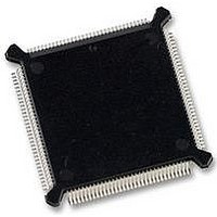
MC68331CEH25 Freescale Semiconductor, MC68331CEH25 Datasheet - Page 240

MC68331CEH25
Manufacturer Part Number
MC68331CEH25
Description
IC MCU 32BIT 25MHZ 132-PQFP
Manufacturer
Freescale Semiconductor
Series
M683xxr
Specifications of MC68331CEH25
Core Processor
CPU32
Core Size
32-Bit
Speed
25MHz
Connectivity
EBI/EMI, SCI, SPI, UART/USART
Peripherals
POR, PWM, WDT
Number Of I /o
18
Program Memory Type
ROMless
Voltage - Supply (vcc/vdd)
4.5 V ~ 5.5 V
Oscillator Type
Internal
Operating Temperature
-40°C ~ 85°C
Package / Case
132-QFP
Controller Family/series
68K
No. Of I/o's
18
Cpu Speed
25MHz
No. Of Timers
1
Embedded Interface Type
QSPI, SCI, UART
No. Of Pwm Channels
2
Digital Ic Case Style
PQFP
Rohs Compliant
Yes
Processor Series
M683xx
Core
CPU32
Data Bus Width
32 bit
Data Ram Size
80 B
Interface Type
QSPI, SCI, UART
Maximum Clock Frequency
25 MHz
Number Of Programmable I/os
18
Number Of Timers
1
Maximum Operating Temperature
+ 85 C
Mounting Style
SMD/SMT
Minimum Operating Temperature
- 40 C
Eeprom Size
-
Ram Size
-
Program Memory Size
-
Data Converters
-
Lead Free Status / Rohs Status
Details
Available stocks
Company
Part Number
Manufacturer
Quantity
Price
Company:
Part Number:
MC68331CEH25
Manufacturer:
PANASONIC
Quantity:
2 000
Company:
Part Number:
MC68331CEH25
Manufacturer:
Freescale Semiconductor
Quantity:
135
Company:
Part Number:
MC68331CEH25
Manufacturer:
Freescale Semiconductor
Quantity:
10 000
- Current page: 240 of 254
- Download datasheet (7Mb)
D
D.4.10 SPCR0 — QSPI Control Register 0
MSTR — Master/Slave Mode Select
D-32
RESET:
MSTR
15
0
DDRQS determines the direction of the TXD pin only when the SCI transmitter is dis-
abled. When the SCI transmitter is enabled, the TXD pin is an output.
SPCR0 contains parameters for configuring the QSPI and enabling various modes of
operation. The CPU has read/write access to SPCR0, but the QSM has read access
only. SPCR0 must be initialized before QSPI operation begins. Writing a new value to
SPCR0 while the QSPI is enabled disrupts operation.
1. PQS2 is a digital I/O pin unless the SPI is enabled (SPE in SPCR1 set), in which case it becomes SPI
2. PQS7 is a digital I/O pin unless the SCI transmitter is enabled (TE in SCCR1 =1), in which case it
0 = QSPI is a slave device.
1 = QSPI is system master.
serial clock SCK.
becomes SCI serial output TXD.
WOMQ
14
0
PCS0/SS
QSM Pin
PCS[3:1]
MISO
MOSI
SCK
TXD
RXD
13
0
Table D-16 Effect of DDRQS on QSM Pin Function
1
2
0
BITS
Freescale Semiconductor, Inc.
For More Information On This Product,
0
Transmit
Receive
Master
Master
Master
Master
Master
Mode
Slave
Slave
Slave
Slave
Slave
10
0
Go to: www.freescale.com
REGISTER SUMMARY
CPOL
9
0
DDRQS
DDQS0
DDQS1
DDQS2
DDQS3
DDQS7
DDQS
None
[4:6]
Bit
CPHA
8
1
State
7
0
NA
Bit
X
0
1
0
1
0
1
0
1
0
1
0
1
0
1
0
1
0
1
0
1
0
Serial Data Input to QSPI
Disables Data Input
Disables Data Output
Serial Data Output from QSPI
Disables Data Output
Serial Data Output from QSPI
Serial Data Input to QSPI
Disables Data Input
Disables Clock Output
Clock Output from QSPI
Clock Input to QSPI
Disables Clock Input
Assertion Causes Mode Fault
Chip-Select Output
QSPI Slave Select Input
Disables Select Input
Disables Chip-Select Output
Chip-Select Output
Inactive
Inactive
Serial Data Output from SCI
Serial Data Input to SCI
0
Pin Function
0
SP
0
USER’S MANUAL
1
$YFFC18
0
MC68331
0
0
Related parts for MC68331CEH25
Image
Part Number
Description
Manufacturer
Datasheet
Request
R
Part Number:
Description:
Mc68331 32 Bit Microcontroller
Manufacturer:
Freescale Semiconductor, Inc
Datasheet:
Part Number:
Description:
Manufacturer:
Freescale Semiconductor, Inc
Datasheet:
Part Number:
Description:
Manufacturer:
Freescale Semiconductor, Inc
Datasheet:
Part Number:
Description:
Manufacturer:
Freescale Semiconductor, Inc
Datasheet:
Part Number:
Description:
Manufacturer:
Freescale Semiconductor, Inc
Datasheet:
Part Number:
Description:
Manufacturer:
Freescale Semiconductor, Inc
Datasheet:
Part Number:
Description:
Manufacturer:
Freescale Semiconductor, Inc
Datasheet:
Part Number:
Description:
Manufacturer:
Freescale Semiconductor, Inc
Datasheet:
Part Number:
Description:
Manufacturer:
Freescale Semiconductor, Inc
Datasheet:
Part Number:
Description:
Manufacturer:
Freescale Semiconductor, Inc
Datasheet:
Part Number:
Description:
Manufacturer:
Freescale Semiconductor, Inc
Datasheet:
Part Number:
Description:
Manufacturer:
Freescale Semiconductor, Inc
Datasheet:
Part Number:
Description:
Manufacturer:
Freescale Semiconductor, Inc
Datasheet:
Part Number:
Description:
Manufacturer:
Freescale Semiconductor, Inc
Datasheet:
Part Number:
Description:
Manufacturer:
Freescale Semiconductor, Inc
Datasheet:


