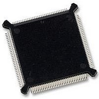
MC68331CEH25 Freescale Semiconductor, MC68331CEH25 Datasheet - Page 170

MC68331CEH25
Manufacturer Part Number
MC68331CEH25
Description
IC MCU 32BIT 25MHZ 132-PQFP
Manufacturer
Freescale Semiconductor
Series
M683xxr
Specifications of MC68331CEH25
Core Processor
CPU32
Core Size
32-Bit
Speed
25MHz
Connectivity
EBI/EMI, SCI, SPI, UART/USART
Peripherals
POR, PWM, WDT
Number Of I /o
18
Program Memory Type
ROMless
Voltage - Supply (vcc/vdd)
4.5 V ~ 5.5 V
Oscillator Type
Internal
Operating Temperature
-40°C ~ 85°C
Package / Case
132-QFP
Controller Family/series
68K
No. Of I/o's
18
Cpu Speed
25MHz
No. Of Timers
1
Embedded Interface Type
QSPI, SCI, UART
No. Of Pwm Channels
2
Digital Ic Case Style
PQFP
Rohs Compliant
Yes
Processor Series
M683xx
Core
CPU32
Data Bus Width
32 bit
Data Ram Size
80 B
Interface Type
QSPI, SCI, UART
Maximum Clock Frequency
25 MHz
Number Of Programmable I/os
18
Number Of Timers
1
Maximum Operating Temperature
+ 85 C
Mounting Style
SMD/SMT
Minimum Operating Temperature
- 40 C
Eeprom Size
-
Ram Size
-
Program Memory Size
-
Data Converters
-
Lead Free Status / Rohs Status
Details
Available stocks
Company
Part Number
Manufacturer
Quantity
Price
Company:
Part Number:
MC68331CEH25
Manufacturer:
PANASONIC
Quantity:
2 000
Company:
Part Number:
MC68331CEH25
Manufacturer:
Freescale Semiconductor
Quantity:
135
Company:
Part Number:
MC68331CEH25
Manufacturer:
Freescale Semiconductor
Quantity:
10 000
- Current page: 170 of 254
- Download datasheet (7Mb)
7
7.8.3 Output Compare Functions
7-12
synchronized with the system clock so that latching of TCNT content and counter in-
crementation occur on opposite half-cycles of the system clock. Inputs have hystere-
sis. Capture of any transition longer than two system clocks is guaranteed; any
transition shorter than one system clock has no effect.
Figure 7-4 shows the relationship of system clock to synchronizer output. The value
latched into the capture register is the value of the counter several system clock cycles
after the transition that triggers the edge detection logic. There can be up to one clock
cycle of uncertainty in latching of the input transition. Maximum time is determined by
the system clock frequency.
The input capture register is a 16-bit register. A word access is required to ensure co-
herency. If coherency is not required, byte accesses can be used to read the register.
Input capture registers can be read at any time without affecting their values.
An input capture occurs every time a selected edge is detected, even when the input
capture status flag is set. This means that the value read from the input capture regis-
ter corresponds to the most recent edge detected, which may not be the edge that
caused the status flag to be set.
Each GPT output compare pin has an associated 16-bit compare register and a 16-bit
comparator. Each output compare function has an associated status flag, and can
cause the GPT to make an interrupt service request. Output compare logic is designed
to prevent false compares during data transition times.
CAPTURE REGISTER
CAPTURE/COMPARE
SYNCHRONIZER
EXTERNAL PIN
F
SYS
ICF FLAG
OUTPUT
CLOCK
TCNT
(PH1)
Figure 7-4 Input Capture Timing Example
Freescale Semiconductor, Inc.
For More Information On This Product,
GENERAL-PURPOSE TIMER
Go to: www.freescale.com
$0101
$0102
$0102
USER’S MANUAL
1153A
MC68331
Related parts for MC68331CEH25
Image
Part Number
Description
Manufacturer
Datasheet
Request
R
Part Number:
Description:
Mc68331 32 Bit Microcontroller
Manufacturer:
Freescale Semiconductor, Inc
Datasheet:
Part Number:
Description:
Manufacturer:
Freescale Semiconductor, Inc
Datasheet:
Part Number:
Description:
Manufacturer:
Freescale Semiconductor, Inc
Datasheet:
Part Number:
Description:
Manufacturer:
Freescale Semiconductor, Inc
Datasheet:
Part Number:
Description:
Manufacturer:
Freescale Semiconductor, Inc
Datasheet:
Part Number:
Description:
Manufacturer:
Freescale Semiconductor, Inc
Datasheet:
Part Number:
Description:
Manufacturer:
Freescale Semiconductor, Inc
Datasheet:
Part Number:
Description:
Manufacturer:
Freescale Semiconductor, Inc
Datasheet:
Part Number:
Description:
Manufacturer:
Freescale Semiconductor, Inc
Datasheet:
Part Number:
Description:
Manufacturer:
Freescale Semiconductor, Inc
Datasheet:
Part Number:
Description:
Manufacturer:
Freescale Semiconductor, Inc
Datasheet:
Part Number:
Description:
Manufacturer:
Freescale Semiconductor, Inc
Datasheet:
Part Number:
Description:
Manufacturer:
Freescale Semiconductor, Inc
Datasheet:
Part Number:
Description:
Manufacturer:
Freescale Semiconductor, Inc
Datasheet:
Part Number:
Description:
Manufacturer:
Freescale Semiconductor, Inc
Datasheet:


