MC68302EH16C Freescale Semiconductor, MC68302EH16C Datasheet - Page 95
MC68302EH16C
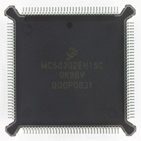
Manufacturer Part Number
MC68302EH16C
Description
IC MPU MULTI-PROTOCOL 132-PQFP
Manufacturer
Freescale Semiconductor
Datasheets
1.MC68302AG20C.pdf
(4 pages)
2.MC68302AG20C.pdf
(2 pages)
3.MC68302AG20C.pdf
(13 pages)
4.MC68302EH16C.pdf
(481 pages)
Specifications of MC68302EH16C
Processor Type
M683xx 32-Bit
Speed
16MHz
Voltage
5V
Mounting Type
Surface Mount
Package / Case
132-MQFP, 132-PQFP
Controller Family/series
68K
Core Size
32 Bit
Ram Memory Size
1152Byte
Cpu Speed
16MHz
No. Of Timers
3
Embedded Interface Type
SCP, TDM
Digital Ic Case Style
PQFP
Rohs Compliant
Yes
Family Name
M68000
Device Core
ColdFire
Device Core Size
32b
Frequency (max)
16MHz
Instruction Set Architecture
RISC
Supply Voltage 1 (typ)
5V
Operating Temp Range
0C to 70C
Operating Temperature Classification
Commercial
Mounting
Surface Mount
Pin Count
132
Package Type
PQFP
Lead Free Status / RoHS Status
Lead free / RoHS Compliant
Features
-
Lead Free Status / Rohs Status
RoHS Compliant part
Electrostatic Device
Available stocks
Company
Part Number
Manufacturer
Quantity
Price
Company:

Part Number:
MC68302EH16C
Manufacturer:
Freescale Semiconductor
Quantity:
135
Company:
Part Number:
MC68302EH16C
Manufacturer:
PANA
Quantity:
99
Company:
Part Number:
MC68302EH16C
Manufacturer:
Freescale Semiconductor
Quantity:
10 000
Part Number:
MC68302EH16C
Manufacturer:
FREESCALE
Quantity:
20 000
Company:
Part Number:
MC68302EH16CB1
Manufacturer:
Freescale Semiconductor
Quantity:
10 000
Company:
Part Number:
MC68302EH16CR2
Manufacturer:
Freescale Semiconductor
Quantity:
10 000


A special case occurs when the locked read-modify-write test and set (TAS) instruction is
executed in combination with the chip selects. The assertion of wait states on the write por-
tion of the cycle will only occur if the RMCST bit in the SCR is set. Refer to 3.8.3 System
Control Bits for more details.
3.6.1 Chip-Select Logic Key Features
Key features of the chip-select logic are as follows:
3.6.2 Chip-Select Registers
Each of the four chip-select units has two registers that define its specific operation. These
registers are a 16-bit base register (BR) and a 16-bit option register (OR) (e.g., BR0 and
OR0). These registers may be modified by the M68000 core. The BR should normally be
programmed after the OR since the BR contains the chip-select enable bit.
3.6.2.1 Base Register (BR3–BR0)
These 16-bit registers consist of a base address field, a read-write bit, and a function code
field.
FC2–FC0 —Function Code Field
MOTOROLA
• Four Programmable Chip-Select Lines
• Various Block Sizes: 8K, 16K, 32K, 64K, 128K, 256K, 512K, 1M, 2M, 4M, 8M, and 16M
• Read-Only, Write-Only, or Read-Write Select
• Internal DTACK Generation with Wait-State Options
• Default Line (CS0) to Select an 8K-Boot ROM Containing the Reset Vector and Initial
This field is contained in bits 15–13 of each BR. These bits are used to set the address
space function code. The address compare logic uses these bits to determine whether an
15
Bytes
Program
FC2 –FC0
SCR), will not activate the chip-select lines. Thus, it is conve-
nient to use one of the chip-select lines to select external ROM/
RAM that overlaps these register addresses, since, in this way,
bus contention is completely avoided during a read access to
these addresses. If, in a given application, it is not possible to
use the chip-select lines for this purpose, the IAC signal may be
used externally to prevent bus contention.
The chip-select logic does not allow an address match during in-
terrupt acknowledge cycles.
13
12
MC68302 USER’S MANUAL
BASE ADDRESS (A23–A13)
NOTE
System Integration Block (SIB)
2
RW
1
3-45
EN
0
Related parts for MC68302EH16C
Image
Part Number
Description
Manufacturer
Datasheet
Request
R

Part Number:
Description:
Manufacturer:
Freescale Semiconductor, Inc
Datasheet:

Part Number:
Description:
MC68302 Configuring the Chip Selects on the MC68302
Manufacturer:
Motorola / Freescale Semiconductor
Part Number:
Description:
MC68302 Design Concept - Expanding Interrupts on the MC68302
Manufacturer:
Motorola / Freescale Semiconductor
Part Number:
Description:
MC68302 MC68302 Adapting a WAN Controller to a LAN Environment
Manufacturer:
Motorola / Freescale Semiconductor
Part Number:
Description:
MC68302 EKB Applications - Power Measurements on the MC68302
Manufacturer:
Motorola / Freescale Semiconductor
Part Number:
Description:
MC68302 Interfacing the MC68020 to a Slave MC68302
Manufacturer:
Motorola / Freescale Semiconductor
Part Number:
Description:
MC68302 MC68302 Software Performance
Manufacturer:
Motorola / Freescale Semiconductor
Part Number:
Description:
MC68302 Evaluating EDX on the ADS302
Manufacturer:
Motorola / Freescale Semiconductor
Part Number:
Description:
MC68302 Design Advisory #1 - MC68SC302 Passive ISDN Protocol Engine
Manufacturer:
Motorola / Freescale Semiconductor
Part Number:
Description:
MC68302, MC68360, and MPC860 Characteristics and Design Notes for Crystal Feedback Oscillators
Manufacturer:
Motorola / Freescale Semiconductor
Part Number:
Description:
Mc68302 Integrated Multi-protocol Processor
Manufacturer:
Freescale Semiconductor, Inc
Datasheet:
Part Number:
Description:
Manufacturer:
Freescale Semiconductor, Inc
Datasheet:
Part Number:
Description:
Manufacturer:
Freescale Semiconductor, Inc
Datasheet:
Part Number:
Description:
Manufacturer:
Freescale Semiconductor, Inc
Datasheet:
Part Number:
Description:
Manufacturer:
Freescale Semiconductor, Inc
Datasheet: