MC68302EH16C Freescale Semiconductor, MC68302EH16C Datasheet - Page 81
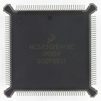
MC68302EH16C
Manufacturer Part Number
MC68302EH16C
Description
IC MPU MULTI-PROTOCOL 132-PQFP
Manufacturer
Freescale Semiconductor
Datasheets
1.MC68302AG20C.pdf
(4 pages)
2.MC68302AG20C.pdf
(2 pages)
3.MC68302AG20C.pdf
(13 pages)
4.MC68302EH16C.pdf
(481 pages)
Specifications of MC68302EH16C
Processor Type
M683xx 32-Bit
Speed
16MHz
Voltage
5V
Mounting Type
Surface Mount
Package / Case
132-MQFP, 132-PQFP
Controller Family/series
68K
Core Size
32 Bit
Ram Memory Size
1152Byte
Cpu Speed
16MHz
No. Of Timers
3
Embedded Interface Type
SCP, TDM
Digital Ic Case Style
PQFP
Rohs Compliant
Yes
Family Name
M68000
Device Core
ColdFire
Device Core Size
32b
Frequency (max)
16MHz
Instruction Set Architecture
RISC
Supply Voltage 1 (typ)
5V
Operating Temp Range
0C to 70C
Operating Temperature Classification
Commercial
Mounting
Surface Mount
Pin Count
132
Package Type
PQFP
Lead Free Status / RoHS Status
Lead free / RoHS Compliant
Features
-
Lead Free Status / Rohs Status
RoHS Compliant part
Electrostatic Device
Available stocks
Company
Part Number
Manufacturer
Quantity
Price
Company:

Part Number:
MC68302EH16C
Manufacturer:
Freescale Semiconductor
Quantity:
135
Company:
Part Number:
MC68302EH16C
Manufacturer:
PANA
Quantity:
99
Company:
Part Number:
MC68302EH16C
Manufacturer:
Freescale Semiconductor
Quantity:
10 000
Part Number:
MC68302EH16C
Manufacturer:
FREESCALE
Quantity:
20 000
Company:
Part Number:
MC68302EH16CB1
Manufacturer:
Freescale Semiconductor
Quantity:
10 000
Company:
Part Number:
MC68302EH16CR2
Manufacturer:
Freescale Semiconductor
Quantity:
10 000


now receives as its input, given that some of its pins have been reassigned, is shown in Ta-
ble 3-6. If an input pin to a channel (for example CD2 or CTS2) is used as a general-purpose
I/O pin, then the input to the peripheral is automatically connected internally to V
based on the pin's function. This does not affect the operation of the port pins in their gen-
eral-purpose I/O function.
3.3.2 Port B
Port B has 12 pins. PB7–PB0 may be configured as general-purpose I/O pins or as dedicat-
ed peripheral interface pins; whereas, PB11–PB8 are always maintained as four general-
purpose pins, each with interrupt capability.
3.3.2.1 PB7–PB0
Each port B pin may be configured as a general-purpose I/O pin or as a dedicated peripheral
interface pin. PB7–PB0 functions exactly like PA15–PA0, except that PB7–PB0 is controlled
by the port B control register (PBCNT), the port B data direction register (PBDDR), and the
port B data register (PBDAT), and PB7 is configured as an open-drain output (WDOG) upon
total system reset.
MOTOROLA
If the DREQ/PA13 pin is selected to be PA13, then DREQ is tied
low. If the IDMA is programmed for external requests, then it al-
ways recognizes an external request, and the entire block will be
transferred in one burst.
# Allows a single external clock source on the RCLK pin to clock both
PACNT Bit = 1
Pin Function
the SCC receiver and transmitter.
SDS2/BRG2
RCLK2
RCLK3
TCLK2
TCLK3
DREQ
DONE
RXD2
RXD3
BRG3
DACK
TXD2
CTS2
RTS2
TXD3
CD2
Table 3-6. Port A Pin Functions
MC68302 USER’S MANUAL
PACNT Bit = 0
Pin Function
PA10
PA11
PA12
PA13
PA14
PA15
PAO
PA1
PA2
PA3
PA4
PA5
PA6
PA7
PA8
PA9
NOTE
SCC2/SCC3/IDMA
Input to
RCLK2 #
RCLK3 #
GND
GND
GND
GND
GND
GND
GND
V DD
—
—
—
—
—
—
System Integration Block (SIB)
DD
or GND,
3-31
Related parts for MC68302EH16C
Image
Part Number
Description
Manufacturer
Datasheet
Request
R

Part Number:
Description:
Manufacturer:
Freescale Semiconductor, Inc
Datasheet:

Part Number:
Description:
MC68302 Configuring the Chip Selects on the MC68302
Manufacturer:
Motorola / Freescale Semiconductor
Part Number:
Description:
MC68302 Design Concept - Expanding Interrupts on the MC68302
Manufacturer:
Motorola / Freescale Semiconductor
Part Number:
Description:
MC68302 MC68302 Adapting a WAN Controller to a LAN Environment
Manufacturer:
Motorola / Freescale Semiconductor
Part Number:
Description:
MC68302 EKB Applications - Power Measurements on the MC68302
Manufacturer:
Motorola / Freescale Semiconductor
Part Number:
Description:
MC68302 Interfacing the MC68020 to a Slave MC68302
Manufacturer:
Motorola / Freescale Semiconductor
Part Number:
Description:
MC68302 MC68302 Software Performance
Manufacturer:
Motorola / Freescale Semiconductor
Part Number:
Description:
MC68302 Evaluating EDX on the ADS302
Manufacturer:
Motorola / Freescale Semiconductor
Part Number:
Description:
MC68302 Design Advisory #1 - MC68SC302 Passive ISDN Protocol Engine
Manufacturer:
Motorola / Freescale Semiconductor
Part Number:
Description:
MC68302, MC68360, and MPC860 Characteristics and Design Notes for Crystal Feedback Oscillators
Manufacturer:
Motorola / Freescale Semiconductor
Part Number:
Description:
Mc68302 Integrated Multi-protocol Processor
Manufacturer:
Freescale Semiconductor, Inc
Datasheet:
Part Number:
Description:
Manufacturer:
Freescale Semiconductor, Inc
Datasheet:
Part Number:
Description:
Manufacturer:
Freescale Semiconductor, Inc
Datasheet:
Part Number:
Description:
Manufacturer:
Freescale Semiconductor, Inc
Datasheet:
Part Number:
Description:
Manufacturer:
Freescale Semiconductor, Inc
Datasheet: