MC68302EH16C Freescale Semiconductor, MC68302EH16C Datasheet - Page 320
MC68302EH16C
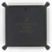
Manufacturer Part Number
MC68302EH16C
Description
IC MPU MULTI-PROTOCOL 132-PQFP
Manufacturer
Freescale Semiconductor
Datasheets
1.MC68302AG20C.pdf
(4 pages)
2.MC68302AG20C.pdf
(2 pages)
3.MC68302AG20C.pdf
(13 pages)
4.MC68302EH16C.pdf
(481 pages)
Specifications of MC68302EH16C
Processor Type
M683xx 32-Bit
Speed
16MHz
Voltage
5V
Mounting Type
Surface Mount
Package / Case
132-MQFP, 132-PQFP
Controller Family/series
68K
Core Size
32 Bit
Ram Memory Size
1152Byte
Cpu Speed
16MHz
No. Of Timers
3
Embedded Interface Type
SCP, TDM
Digital Ic Case Style
PQFP
Rohs Compliant
Yes
Family Name
M68000
Device Core
ColdFire
Device Core Size
32b
Frequency (max)
16MHz
Instruction Set Architecture
RISC
Supply Voltage 1 (typ)
5V
Operating Temp Range
0C to 70C
Operating Temperature Classification
Commercial
Mounting
Surface Mount
Pin Count
132
Package Type
PQFP
Lead Free Status / RoHS Status
Lead free / RoHS Compliant
Features
-
Lead Free Status / Rohs Status
RoHS Compliant part
Electrostatic Device
Available stocks
Company
Part Number
Manufacturer
Quantity
Price
Company:

Part Number:
MC68302EH16C
Manufacturer:
Freescale Semiconductor
Quantity:
135
Company:
Part Number:
MC68302EH16C
Manufacturer:
PANA
Quantity:
99
Company:
Part Number:
MC68302EH16C
Manufacturer:
Freescale Semiconductor
Quantity:
10 000
Part Number:
MC68302EH16C
Manufacturer:
FREESCALE
Quantity:
20 000
Company:
Part Number:
MC68302EH16CB1
Manufacturer:
Freescale Semiconductor
Quantity:
10 000
Company:
Part Number:
MC68302EH16CR2
Manufacturer:
Freescale Semiconductor
Quantity:
10 000


Electrical Characteristics
6.20 AC ELECTRICAL SPECIFICATIONS—GCI TIMING
GCI supports the NORMAL mode and the GCI channel 0 (GCN0) in MUX mode. Normal
mode uses 512 kHz clock rate (256K bit rate). MUX mode uses 256 x n - 3088 kbs (clock
rate is data rate x 2). The ratio CLKO/L1CLK must be greater than 2.5/1 (see Figure 6-21).
6-32
NOTES:
1.The ratio CLKO/L1CLK must be greater than 2.5/1.
2. Condition C L = 150 pF. L1TD becomes valid after the L1CLK rising edge or L1SY1, whichever is later.
3.SDS1–SDS2 become valid after the L1CLK rising edge or L1SY1, whichever is later.
4.Schmitt trigger used on input buffer.
5.Where P = 1/CLKO. Thus, for a 16.67-MHz CLKO rate, P = 60 ns.
Num.
281A
280
281
282
280
281
282
283
284
285
286
287
288
289
290
291
292
293
L1CLK GCI Clock Frequency (Normal Mode) (see
Note 1)
L1CLK Clock Period Normal Mode (see Note 1)
L1CLK Width Low/High Normal Mode
L1CLK Rise/Fall Time Normal Mode (see Note 4)
L1CLK (GCI Clock) Frequency (MUX Mode) (see
Note 1)
L1CLK Clock Period MUX Mode (see Note 1)
L1CLK Width Low MUX Mode
L1CLK Width High MUX Mode (see Note 5)
L1CLK Rise/Fall Time MUX Mode (see Note 4)
L1SY1 Sync Setup Time to L1CLK Falling Edge
L1SY1 Sync Hold Time from L1CLK Falling Edge
L1TxD Active Delay (from L1CLK Rising Edge) (see
Note 2)
L1TxD Active Delay (from L1SY1 Rising Edge) (see
Note 2)
L1RxD Setup Time to L1CLK Rising Edge
L1RxD Hold Time from L1CLK Rising Edge
Time Between Successive L1SY1in
SDS1–SDS2 Active Delay from L1CLK Rising Edge
(see Note 3)
SDS1–SDS2 Active Delay from L1SY1 Rising Edge
(see Note 3)
SDS1–SDS2 Inactive Delay from L1CLK Falling
Edge
GCIDCL (GCI Data Clock) Active Delay
Characteristic
MC68302 USER’S MANUAL
SCIT Mode
Normal
P+10
1800 2100 1800 2100 1800
Min
192
16.67 MHz
840
150
—
—
—
—
64
55
30
50
20
50
10
10
10
0
0
0
6.668
1450
Max
512
100
100
—
—
—
—
—
—
—
—
—
—
—
90
90
90
50
P+10
Min
192
840
150
—
—
—
—
64
20 MHz
55
25
42
17
42
10
10
10
0
0
0
6.668
1450
Max
512
—
—
—
—
—
—
—
—
—
—
—
85
85
75
75
75
42
P+10
Min
192
840
150
—
—
—
—
64
55
20
34
14
34
25 MHz
7
7
7
0
0
0
6.668
2100
1450
Max
512
—
—
—
—
—
—
—
—
—
—
—
70
60
34
70
60
60
MOTOROLA
L1CLK
L1CLK
MHz
Unit
kHz
ns
ns
ns
ns
ns
ns
ns
ns
ns
ns
ns
ns
ns
ns
ns
ns
ns
Related parts for MC68302EH16C
Image
Part Number
Description
Manufacturer
Datasheet
Request
R

Part Number:
Description:
Manufacturer:
Freescale Semiconductor, Inc
Datasheet:

Part Number:
Description:
MC68302 Configuring the Chip Selects on the MC68302
Manufacturer:
Motorola / Freescale Semiconductor
Part Number:
Description:
MC68302 Design Concept - Expanding Interrupts on the MC68302
Manufacturer:
Motorola / Freescale Semiconductor
Part Number:
Description:
MC68302 MC68302 Adapting a WAN Controller to a LAN Environment
Manufacturer:
Motorola / Freescale Semiconductor
Part Number:
Description:
MC68302 EKB Applications - Power Measurements on the MC68302
Manufacturer:
Motorola / Freescale Semiconductor
Part Number:
Description:
MC68302 Interfacing the MC68020 to a Slave MC68302
Manufacturer:
Motorola / Freescale Semiconductor
Part Number:
Description:
MC68302 MC68302 Software Performance
Manufacturer:
Motorola / Freescale Semiconductor
Part Number:
Description:
MC68302 Evaluating EDX on the ADS302
Manufacturer:
Motorola / Freescale Semiconductor
Part Number:
Description:
MC68302 Design Advisory #1 - MC68SC302 Passive ISDN Protocol Engine
Manufacturer:
Motorola / Freescale Semiconductor
Part Number:
Description:
MC68302, MC68360, and MPC860 Characteristics and Design Notes for Crystal Feedback Oscillators
Manufacturer:
Motorola / Freescale Semiconductor
Part Number:
Description:
Mc68302 Integrated Multi-protocol Processor
Manufacturer:
Freescale Semiconductor, Inc
Datasheet:
Part Number:
Description:
Manufacturer:
Freescale Semiconductor, Inc
Datasheet:
Part Number:
Description:
Manufacturer:
Freescale Semiconductor, Inc
Datasheet:
Part Number:
Description:
Manufacturer:
Freescale Semiconductor, Inc
Datasheet:
Part Number:
Description:
Manufacturer:
Freescale Semiconductor, Inc
Datasheet: