MC68302EH16C Freescale Semiconductor, MC68302EH16C Datasheet - Page 401
MC68302EH16C
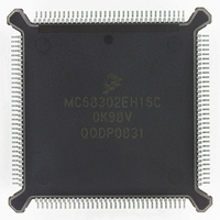
Manufacturer Part Number
MC68302EH16C
Description
IC MPU MULTI-PROTOCOL 132-PQFP
Manufacturer
Freescale Semiconductor
Datasheets
1.MC68302AG20C.pdf
(4 pages)
2.MC68302AG20C.pdf
(2 pages)
3.MC68302AG20C.pdf
(13 pages)
4.MC68302EH16C.pdf
(481 pages)
Specifications of MC68302EH16C
Processor Type
M683xx 32-Bit
Speed
16MHz
Voltage
5V
Mounting Type
Surface Mount
Package / Case
132-MQFP, 132-PQFP
Controller Family/series
68K
Core Size
32 Bit
Ram Memory Size
1152Byte
Cpu Speed
16MHz
No. Of Timers
3
Embedded Interface Type
SCP, TDM
Digital Ic Case Style
PQFP
Rohs Compliant
Yes
Family Name
M68000
Device Core
ColdFire
Device Core Size
32b
Frequency (max)
16MHz
Instruction Set Architecture
RISC
Supply Voltage 1 (typ)
5V
Operating Temp Range
0C to 70C
Operating Temperature Classification
Commercial
Mounting
Surface Mount
Pin Count
132
Package Type
PQFP
Lead Free Status / RoHS Status
Lead free / RoHS Compliant
Features
-
Lead Free Status / Rohs Status
RoHS Compliant part
Electrostatic Device
Available stocks
Company
Part Number
Manufacturer
Quantity
Price
Company:

Part Number:
MC68302EH16C
Manufacturer:
Freescale Semiconductor
Quantity:
135
Company:
Part Number:
MC68302EH16C
Manufacturer:
PANA
Quantity:
99
Company:
Part Number:
MC68302EH16C
Manufacturer:
Freescale Semiconductor
Quantity:
10 000
Part Number:
MC68302EH16C
Manufacturer:
FREESCALE
Quantity:
20 000
Company:
Part Number:
MC68302EH16CB1
Manufacturer:
Freescale Semiconductor
Quantity:
10 000
Company:
Part Number:
MC68302EH16CR2
Manufacturer:
Freescale Semiconductor
Quantity:
10 000


MC68302 Applications
of the physical interface configuration. Similarly, all bits in the receive buffer will be filled with
real transparent data (full packing is always performed), regardless of the physical interface
configuration.
If no data is available to transmit, transparent mode will transmit ones. The decision of
whether to set the last (L) bit in the Tx BD is left to the user. If multiple buffers are to be sent
back-to-back with no gaps in between, the L bit should be cleared in all buffers except for
the last buffer. In this case, failure to provide buffers in time will result in a transmit underrun.
If the L bit is set, the frame will end without error, and the transmission of ones will resume.
The transmit byte count and buffer alignment need not be even, but the SDMA channel will
always read words on an even-byte boundary, even if it has to discard one of the two bytes.
For example, if a transmit buffer begins on an odd-byte boundary and is 10 bytes in length
(worst case), six word reads will result, even though only 10 bytes will be transmitted.
The receive buffer length (stored in MRBLR) and starting address must be even. All trans-
fers to memory will be of word length and, unless an error occurs, a buffer will not be closed
until it contains MRBLR/two words (the byte count will be equal to MRBLR). This raises an
important point. Data received will only be transmitted to memory every 16 clocks. If a non-
multiple of 16 bits is sent in a frame, the residue bits will not be transmitted to memory until
additional bits arrive, and it will be impossible to demarcate frames unless their length is pre-
determined. (If a SYNC character is received with the data, the BISYNC mode can be used
to receive an odd number of bytes with odd-length receive buffers and pointers allowed. (For
more detailed information, refer to D.8.6 Other NMSI Modes.)
When the enable transmitter (ENT) bit is set, the process of polling the Tx BD begins by the
RISC. The frequency of this polling is determined by the SCC's transmit clock. If the clock
is stopped, no polling will occur. When the ready bit of the first Tx BD is set, the RISC ini-
tiates the SDMA activity of filling up the transmit FIFO with three words of data. Once the
FIFO is full, the RTS signal is asserted, and the physical interface signals take control to de-
termine the exact timing of the transmitted data. Once the physical interface says “go”, typ-
ically one final $FF is transmitted before data begins; however, whether $FF is transmitted
depends on the mode chosen.
When the enable receiver (ENR) bit is set and 16 bits of valid data (as defined by the phys-
ical interface signals) have been clocked into the receiver, the RISC checks to see if the first
receive buffer is available and, if the buffer is available, begins moving the data to it. The
receive FIFO is three words deep, but a single open entry in the FIFO causes an SDMA ser-
vice request. There are three types of receive errors: overrun (receive FIFO overflow), busy
(new data arrived without a receive buffer being available), and CD lost (which is not possi-
ble in any example configuration discussed in this appendix). These errors are reported in
the SCC event register (SCCE) or the Rx BD.
Whenever a buffer has been transmitted with the interrupt (I) bit set in the Tx BD, the TX
event in the SCCE register will be set. This TX bit can cause an interrupt if the corresponding
bit in the SCCM is set. Similarly, whenever a buffer has been received with the interrupt (I)
bit set in the Rx BD, the RX event in the SCCE register will be set. Also, whenever a word
of data is written to the receive buffer, the RCH bit is set in the SCCE.
MOTOROLA
MC68302 USER’S MANUAL
D-51
Related parts for MC68302EH16C
Image
Part Number
Description
Manufacturer
Datasheet
Request
R

Part Number:
Description:
Manufacturer:
Freescale Semiconductor, Inc
Datasheet:

Part Number:
Description:
MC68302 Configuring the Chip Selects on the MC68302
Manufacturer:
Motorola / Freescale Semiconductor
Part Number:
Description:
MC68302 Design Concept - Expanding Interrupts on the MC68302
Manufacturer:
Motorola / Freescale Semiconductor
Part Number:
Description:
MC68302 MC68302 Adapting a WAN Controller to a LAN Environment
Manufacturer:
Motorola / Freescale Semiconductor
Part Number:
Description:
MC68302 EKB Applications - Power Measurements on the MC68302
Manufacturer:
Motorola / Freescale Semiconductor
Part Number:
Description:
MC68302 Interfacing the MC68020 to a Slave MC68302
Manufacturer:
Motorola / Freescale Semiconductor
Part Number:
Description:
MC68302 MC68302 Software Performance
Manufacturer:
Motorola / Freescale Semiconductor
Part Number:
Description:
MC68302 Evaluating EDX on the ADS302
Manufacturer:
Motorola / Freescale Semiconductor
Part Number:
Description:
MC68302 Design Advisory #1 - MC68SC302 Passive ISDN Protocol Engine
Manufacturer:
Motorola / Freescale Semiconductor
Part Number:
Description:
MC68302, MC68360, and MPC860 Characteristics and Design Notes for Crystal Feedback Oscillators
Manufacturer:
Motorola / Freescale Semiconductor
Part Number:
Description:
Mc68302 Integrated Multi-protocol Processor
Manufacturer:
Freescale Semiconductor, Inc
Datasheet:
Part Number:
Description:
Manufacturer:
Freescale Semiconductor, Inc
Datasheet:
Part Number:
Description:
Manufacturer:
Freescale Semiconductor, Inc
Datasheet:
Part Number:
Description:
Manufacturer:
Freescale Semiconductor, Inc
Datasheet:
Part Number:
Description:
Manufacturer:
Freescale Semiconductor, Inc
Datasheet: