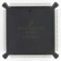
MC68302EH16C Freescale Semiconductor, MC68302EH16C Datasheet - Page 379

MC68302EH16C
Manufacturer Part Number
MC68302EH16C
Description
IC MPU MULTI-PROTOCOL 132-PQFP
Manufacturer
Freescale Semiconductor
Datasheets
1.MC68302AG20C.pdf
(4 pages)
2.MC68302AG20C.pdf
(2 pages)
3.MC68302AG20C.pdf
(13 pages)
4.MC68302EH16C.pdf
(481 pages)
Specifications of MC68302EH16C
Processor Type
M683xx 32-Bit
Speed
16MHz
Voltage
5V
Mounting Type
Surface Mount
Package / Case
132-MQFP, 132-PQFP
Controller Family/series
68K
Core Size
32 Bit
Ram Memory Size
1152Byte
Cpu Speed
16MHz
No. Of Timers
3
Embedded Interface Type
SCP, TDM
Digital Ic Case Style
PQFP
Rohs Compliant
Yes
Family Name
M68000
Device Core
ColdFire
Device Core Size
32b
Frequency (max)
16MHz
Instruction Set Architecture
RISC
Supply Voltage 1 (typ)
5V
Operating Temp Range
0C to 70C
Operating Temperature Classification
Commercial
Mounting
Surface Mount
Pin Count
132
Package Type
PQFP
Lead Free Status / RoHS Status
Lead free / RoHS Compliant
Features
-
Lead Free Status / Rohs Status
RoHS Compliant part
Electrostatic Device
Available stocks
Company
Part Number
Manufacturer
Quantity
Price
Company:
Part Number:
MC68302EH16C
Manufacturer:
Freescale Semiconductor
Quantity:
135
Company:
Part Number:
MC68302EH16C
Manufacturer:
PANA
Quantity:
99
Company:
Part Number:
MC68302EH16C
Manufacturer:
Freescale Semiconductor
Quantity:
10 000
Part Number:
MC68302EH16C
Manufacturer:
FREESCALE
Quantity:
20 000
Company:
Part Number:
MC68302EH16CB1
Manufacturer:
Freescale Semiconductor
Quantity:
10 000
Company:
Part Number:
MC68302EH16CR2
Manufacturer:
Freescale Semiconductor
Quantity:
10 000
- MC68302AG20C PDF datasheet
- MC68302AG20C PDF datasheet #2
- MC68302AG20C PDF datasheet #3
- MC68302EH16C PDF datasheet #4
- Current page: 379 of 481
- Download datasheet (2Mb)
Figure D-10 illustrates the activation of external burst mode by using the DREQ signal as a
level-sensitive input to the IDMA. If DREQ is asserted when the IDMA is accessing the pe-
ripheral (indicated by DACK being asserted) as shown in Figure D-10, then the IDMA will
continue servicing the peripheral by performing another sequence of operand transfer cy-
cles. The external burst mode stops when the DREQ signal is deasserted prior to the trailing
edge of S3 in the cycle where DACK is asserted.
D.5.7 Internal Interrupt Sequence
An interrupt acknowledge cycle (IACK) occurs when an allowed internal or external interrupt
request is pending and the priority of the interrupt is higher than the current microprocessor
run level. The interrupt acknowledge cycle begins at the conclusion of instruction execution
in state S0. All internal resources, including the IDMA, generate INRQ requests at level 4.
The four registers used in interrupt processing are as follows:
A level 4 interrupt may be generated by the IDMA upon completion of a data block transfer.
Interrupt processing of IDMA transfers is possible by 1) setting the IDMA interrupt enable
(bit 11) in the IMR and 2) setting one or both interrupt enable (INTN and INTE) bits in the
CMR (see Table D-1). Once in the interrupt handler, four bits in the CSR indicate the reason
for termination of an IDMA data block (see Table D-2).
MOTOROLA
DTACK
NOTE:
LEGEND:
1. The interrupt mask register (IMR) contains the flags that, when set, allow the INRQ
2. The interrupt pending register (IPR) contains bits that correspond to the INRQ source
3. The interrupt in-service register (ISR) indicates which internal interrupts are currently
4. The global interrupt mode register (GIMR) has bits that specify interrupt modes such
DREQ
CLKO
DACK
AS
1
2
source to initiate service.
requesting service.
being processed (usually only one at a time).
as the edge or level of an input that triggers an interrupt.
DREQ asserted prior to DTACK = continue burst mode transfer
DREQ negated prior to DTACK = relinquish the bus
DREQ is sampled on the falling edge of clock.
S0 S1
READ CYCLE
S2
S3 S4 S5 S6 S7
Figure D-10. Burst Mode Cycles
MC68302 USER’S MANUAL
WRITE CYCLE
1
READ CYCLE
MC68302 Applications
2
WRITE CYCLE
D-29
Related parts for MC68302EH16C
Image
Part Number
Description
Manufacturer
Datasheet
Request
R
Part Number:
Description:
Manufacturer:
Freescale Semiconductor, Inc
Datasheet:

Part Number:
Description:
MC68302 Configuring the Chip Selects on the MC68302
Manufacturer:
Motorola / Freescale Semiconductor

Part Number:
Description:
MC68302 Design Concept - Expanding Interrupts on the MC68302
Manufacturer:
Motorola / Freescale Semiconductor

Part Number:
Description:
MC68302 MC68302 Adapting a WAN Controller to a LAN Environment
Manufacturer:
Motorola / Freescale Semiconductor

Part Number:
Description:
MC68302 EKB Applications - Power Measurements on the MC68302
Manufacturer:
Motorola / Freescale Semiconductor

Part Number:
Description:
MC68302 Interfacing the MC68020 to a Slave MC68302
Manufacturer:
Motorola / Freescale Semiconductor

Part Number:
Description:
MC68302 MC68302 Software Performance
Manufacturer:
Motorola / Freescale Semiconductor

Part Number:
Description:
MC68302 Evaluating EDX on the ADS302
Manufacturer:
Motorola / Freescale Semiconductor

Part Number:
Description:
MC68302 Design Advisory #1 - MC68SC302 Passive ISDN Protocol Engine
Manufacturer:
Motorola / Freescale Semiconductor

Part Number:
Description:
MC68302, MC68360, and MPC860 Characteristics and Design Notes for Crystal Feedback Oscillators
Manufacturer:
Motorola / Freescale Semiconductor
Part Number:
Description:
Mc68302 Integrated Multi-protocol Processor
Manufacturer:
Freescale Semiconductor, Inc
Datasheet:
Part Number:
Description:
Manufacturer:
Freescale Semiconductor, Inc
Datasheet:
Part Number:
Description:
Manufacturer:
Freescale Semiconductor, Inc
Datasheet:
Part Number:
Description:
Manufacturer:
Freescale Semiconductor, Inc
Datasheet:
Part Number:
Description:
Manufacturer:
Freescale Semiconductor, Inc
Datasheet:


