MC68302EH16C Freescale Semiconductor, MC68302EH16C Datasheet - Page 280
MC68302EH16C
Manufacturer Part Number
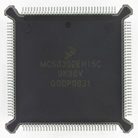
MC68302EH16C
Description
IC MPU MULTI-PROTOCOL 132-PQFP
Manufacturer
Freescale Semiconductor
Datasheets
1.MC68302AG20C.pdf
(4 pages)
2.MC68302AG20C.pdf
(2 pages)
3.MC68302AG20C.pdf
(13 pages)
4.MC68302EH16C.pdf
(481 pages)
Specifications of MC68302EH16C
Processor Type
M683xx 32-Bit
Speed
16MHz
Voltage
5V
Mounting Type
Surface Mount
Package / Case
132-MQFP, 132-PQFP
Controller Family/series
68K
Core Size
32 Bit
Ram Memory Size
1152Byte
Cpu Speed
16MHz
No. Of Timers
3
Embedded Interface Type
SCP, TDM
Digital Ic Case Style
PQFP
Rohs Compliant
Yes
Family Name
M68000
Device Core
ColdFire
Device Core Size
32b
Frequency (max)
16MHz
Instruction Set Architecture
RISC
Supply Voltage 1 (typ)
5V
Operating Temp Range
0C to 70C
Operating Temperature Classification
Commercial
Mounting
Surface Mount
Pin Count
132
Package Type
PQFP
Lead Free Status / RoHS Status
Lead free / RoHS Compliant
Features
-
Lead Free Status / Rohs Status
RoHS Compliant part
Electrostatic Device
Available stocks
Company
Part Number
Manufacturer
Quantity
Price
Company:

Part Number:
MC68302EH16C
Manufacturer:
Freescale Semiconductor
Quantity:
135
Company:
Part Number:
MC68302EH16C
Manufacturer:
PANA
Quantity:
99
Company:
Part Number:
MC68302EH16C
Manufacturer:
Freescale Semiconductor
Quantity:
10 000
Part Number:
MC68302EH16C
Manufacturer:
FREESCALE
Quantity:
20 000
Company:
Part Number:
MC68302EH16CB1
Manufacturer:
Freescale Semiconductor
Quantity:
10 000
Company:
Part Number:
MC68302EH16CR2
Manufacturer:
Freescale Semiconductor
Quantity:
10 000


Signal Description
In PCM mode, L1SY1–L1SY0 are encoded signals used to create channels that can be in-
dependently routed to the SCCs.
In IDL/GCI modes, the SDS2–SDS1 outputs may be used to route the B1 and/or B2 chan-
nels to devices that do not support the IDL or GCI buses. This is configured in the serial in-
terface mode (SIMODE) and serial interface mask (SIMASK) registers.
CD1/L1SY1—Carrier Detect/Layer-1 Sync
CTS1/L1GR—Clear to Send/Layer-1 Grant
5-16
This input is used as the NMSI1 carrier detect (CD) pin in NMSI mode, as a PCM sync
signal in PCM mode, and as an L1SYNC signal in IDL/GCI modes.
If the CD1 pin has changed for more than one receive clock cycle, the IMP asserts the
appropriate bit in the SCC1 event register. If the SCC1 channel is programmed not to sup-
port CD1 automatically (in the SCC1 mode register), then this pin may be used as an ex-
ternal interrupt source. The current value of CD1 may be read in the SCCS1 register. See
4.5.8.3 SCC Status Register (SCCs) for details. CD1 may also be used as an external
sync in NMSI mode.
This input is the NMSI1 CTS signal in the NMSI mode or the grant signal in the IDL/GCI
mode. If this pin is not used as a grant signal in GCI mode, it should be connected to V
If the CTS1 pin has changed for more than one transmit clock cycle, the IMP asserts the
appropriate bit in the SCC1 event register and optionally aborts the transmission of that
frame.
When using SCC1 in the NMSI mode with the internal baud rate
generator operating, the TCLK1 and RCLK1 pins will always out-
put the baud rate generator clock unless disabled in the CKCR
register. Thus, if a dynamic selection between an internal and
external clock source is required in an application, the clock pins
should be disabled first in the CKCR register before switching
the TCLK1 and RCLK1 lines. On SCC2 and SCC3, contention
may be avoided by disabling the clock line outputs in the PACNT
register.
NOTE: CH-1, 2, and 3 are connected to the SCCs as determined in the
L1SY1
0
0
1
1
SIMODE register.
Table 5-8. PCM Mode Signals
L1SY0
0
1
0
1
MC68302 USER’S MANUAL
L1TXD is Three-Stated, L1RXD is Ignored
CH-1
CH-2
CH-3
Data (L1RXD, L1TXD) is Routed to SCC
NOTE
MOTOROLA
DD
.
Related parts for MC68302EH16C
Image
Part Number
Description
Manufacturer
Datasheet
Request
R

Part Number:
Description:
Manufacturer:
Freescale Semiconductor, Inc
Datasheet:

Part Number:
Description:
MC68302 Configuring the Chip Selects on the MC68302
Manufacturer:
Motorola / Freescale Semiconductor
Part Number:
Description:
MC68302 Design Concept - Expanding Interrupts on the MC68302
Manufacturer:
Motorola / Freescale Semiconductor
Part Number:
Description:
MC68302 MC68302 Adapting a WAN Controller to a LAN Environment
Manufacturer:
Motorola / Freescale Semiconductor
Part Number:
Description:
MC68302 EKB Applications - Power Measurements on the MC68302
Manufacturer:
Motorola / Freescale Semiconductor
Part Number:
Description:
MC68302 Interfacing the MC68020 to a Slave MC68302
Manufacturer:
Motorola / Freescale Semiconductor
Part Number:
Description:
MC68302 MC68302 Software Performance
Manufacturer:
Motorola / Freescale Semiconductor
Part Number:
Description:
MC68302 Evaluating EDX on the ADS302
Manufacturer:
Motorola / Freescale Semiconductor
Part Number:
Description:
MC68302 Design Advisory #1 - MC68SC302 Passive ISDN Protocol Engine
Manufacturer:
Motorola / Freescale Semiconductor
Part Number:
Description:
MC68302, MC68360, and MPC860 Characteristics and Design Notes for Crystal Feedback Oscillators
Manufacturer:
Motorola / Freescale Semiconductor
Part Number:
Description:
Mc68302 Integrated Multi-protocol Processor
Manufacturer:
Freescale Semiconductor, Inc
Datasheet:
Part Number:
Description:
Manufacturer:
Freescale Semiconductor, Inc
Datasheet:
Part Number:
Description:
Manufacturer:
Freescale Semiconductor, Inc
Datasheet:
Part Number:
Description:
Manufacturer:
Freescale Semiconductor, Inc
Datasheet:
Part Number:
Description:
Manufacturer:
Freescale Semiconductor, Inc
Datasheet: