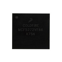
MCF5272VF66 Freescale, MCF5272VF66 Datasheet - Page 87

MCF5272VF66
Manufacturer Part Number
MCF5272VF66
Description
Manufacturer
Freescale
Datasheet
1.MCF5272VF66.pdf
(544 pages)
Specifications of MCF5272VF66
Family Name
MCF5xxx
Device Core
ColdFire
Device Core Size
32b
Frequency (max)
66MHz
Instruction Set Architecture
RISC
Supply Voltage 1 (typ)
3.3V
Operating Temp Range
0C to 70C
Operating Temperature Classification
Commercial
Mounting
Surface Mount
Pin Count
196
Package Type
MA-BGA
Lead Free Status / RoHS Status
Not Compliant
Available stocks
Company
Part Number
Manufacturer
Quantity
Price
Company:
Part Number:
MCF5272VF66
Manufacturer:
HYNIX
Quantity:
19
Company:
Part Number:
MCF5272VF66
Manufacturer:
FREESCAL
Quantity:
885
Company:
Part Number:
MCF5272VF66
Manufacturer:
Freescale Semiconductor
Quantity:
10 000
Part Number:
MCF5272VF66
Manufacturer:
FREESCALE
Quantity:
20 000
Company:
Part Number:
MCF5272VF66J
Manufacturer:
Freescale
Quantity:
256
Company:
Part Number:
MCF5272VF66J
Manufacturer:
Freescale Semiconductor
Quantity:
10 000
Company:
Part Number:
MCF5272VF66R2
Manufacturer:
Freescale Semiconductor
Quantity:
10 000
Company:
Part Number:
MCF5272VF66R2J
Manufacturer:
Freescale Semiconductor
Quantity:
10 000
- Current page: 87 of 544
- Download datasheet (7Mb)
2.7
The timing data presented in this section assumes the following:
Freescale Semiconductor
•
•
•
•
The OEP is loaded with the opword and all required extension words at the beginning of each
instruction execution. This implies that the OEP spends no time waiting for the IFP to supply
opwords and/or extension words.
The OEP experiences no sequence-related pipeline stalls. For the MCF5272,the most common
example of this type of stall involves consecutive store operations, excluding the MOVEM
instruction. For all store operations (except MOVEM), certain hardware resources within the
processor are marked as busy for two clock cycles after the final DSOC cycle of the store
instruction. If a subsequent store instruction is encountered within this two-cycle window, it is
stalled until the resource again becomes available. Thus, the maximum pipeline stall involving
consecutive store operations is two cycles.
The OEP can complete all memory accesses without memory causing any stall conditions. Thus,
timing details in this section assume an infinite zero-wait state memory attached to the core.
All operand data accesses are assumed to be aligned on the same byte boundary as the operand size:
— 16-bit operands aligned on 0-modulo-2 addresses
— 32-bit operands aligned on 0-modulo-4 addresses
Operands that do not meet these guidelines are misaligned.
decomposes a misaligned operand reference into a series of aligned accesses.
1
Instruction Timing
Each timing entry is presented as C(r/w), described as follows:
C is the number of processor clock cycles, including all applicable operand fetches and writes, as
well as all internal core cycles required to complete the instruction execution.
r/w is the number of operand reads (r) and writes (w) required by the instruction. An operation
performing a read-modify write function is denoted as (1/1).
A[1:0]
10
x1
x1
MCF5272 ColdFire
Table 2-9. Misaligned Operand References
Word
Long
Long
Size
®
Integrated Microprocessor User’s Manual, Rev. 3
Byte, Byte
Byte, Word, Byte
Word, Word
Bus Operations
Table 2-9
2(1/0) if read
1(0/1) if write
3(2/0) if read
2(0/2) if write
2(1/0) if read
1(0/1) if write
Additional C(R/W)
shows how the core
1
ColdFire Core
2-19
Related parts for MCF5272VF66
Image
Part Number
Description
Manufacturer
Datasheet
Request
R
Part Number:
Description:
Mcf5272 Coldfire Integrated Microprocessor User
Manufacturer:
Freescale Semiconductor, Inc
Datasheet:

Part Number:
Description:
MCF5272 Interrupt Service Routine for the Physical Layer Interface Controller
Manufacturer:
Freescale Semiconductor / Motorola
Datasheet:

Part Number:
Description:
TOWER ELEVATOR BOARDS HARDWARE
Manufacturer:
Freescale Semiconductor
Datasheet:

Part Number:
Description:
TOWER SERIAL I/O HARDWARE
Manufacturer:
Freescale Semiconductor
Datasheet:

Part Number:
Description:
LCD MODULE FOR TWR SYSTEM
Manufacturer:
Freescale Semiconductor
Datasheet:

Part Number:
Description:
DAUGHTER LCD WVGA I.MX51
Manufacturer:
Freescale Semiconductor
Datasheet:

Part Number:
Description:
TOWER SYSTEM BOARD MPC5125
Manufacturer:
Freescale Semiconductor
Datasheet:

Part Number:
Description:
KIT EVALUATION I.MX51
Manufacturer:
Freescale Semiconductor
Datasheet:

Part Number:
Description:
KIT DEVELOPMENT WINCE IMX25
Manufacturer:
Freescale Semiconductor
Datasheet:

Part Number:
Description:
TOWER SYSTEM KIT MPC5125
Manufacturer:
Freescale Semiconductor
Datasheet:

Part Number:
Description:
TOWER SYSTEM BOARD K40X256
Manufacturer:
Freescale Semiconductor
Datasheet:

Part Number:
Description:
TOWER SYSTEM KIT K40X256
Manufacturer:
Freescale Semiconductor
Datasheet:

Part Number:
Description:
Microcontrollers (MCU) MX28 PLATFORM DEV KIT
Manufacturer:
Freescale Semiconductor
Datasheet:

Part Number:
Description:
MCU, MPU & DSP Development Tools IAR KickStart Kit for Kinetis K60
Manufacturer:
Freescale Semiconductor
Datasheet:

Part Number:
Description:
24BIT HDMI MX535/08
Manufacturer:
Freescale Semiconductor
Datasheet:


