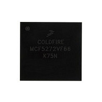
MCF5272VF66 Freescale, MCF5272VF66 Datasheet - Page 419

MCF5272VF66
Manufacturer Part Number
MCF5272VF66
Description
Manufacturer
Freescale
Datasheet
1.MCF5272VF66.pdf
(544 pages)
Specifications of MCF5272VF66
Family Name
MCF5xxx
Device Core
ColdFire
Device Core Size
32b
Frequency (max)
66MHz
Instruction Set Architecture
RISC
Supply Voltage 1 (typ)
3.3V
Operating Temp Range
0C to 70C
Operating Temperature Classification
Commercial
Mounting
Surface Mount
Pin Count
196
Package Type
MA-BGA
Lead Free Status / RoHS Status
Not Compliant
Available stocks
Company
Part Number
Manufacturer
Quantity
Price
Company:
Part Number:
MCF5272VF66
Manufacturer:
HYNIX
Quantity:
19
Company:
Part Number:
MCF5272VF66
Manufacturer:
FREESCAL
Quantity:
885
Company:
Part Number:
MCF5272VF66
Manufacturer:
Freescale Semiconductor
Quantity:
10 000
Part Number:
MCF5272VF66
Manufacturer:
FREESCALE
Quantity:
20 000
Company:
Part Number:
MCF5272VF66J
Manufacturer:
Freescale
Quantity:
256
Company:
Part Number:
MCF5272VF66J
Manufacturer:
Freescale Semiconductor
Quantity:
10 000
Company:
Part Number:
MCF5272VF66R2
Manufacturer:
Freescale Semiconductor
Quantity:
10 000
Company:
Part Number:
MCF5272VF66R2J
Manufacturer:
Freescale Semiconductor
Quantity:
10 000
- Current page: 419 of 544
- Download datasheet (7Mb)
Freescale Semiconductor
(see notes)
Configured
MTMOD
MTMOD
MTMOD
MTMOD
by
4
4
4
4
1
PWM_OUT0
QSPI_Dout/
QSPI_CLK/
QSPI_CS0/
QSPI_Din
0 (Reset)
SDCLKE
BYPASS
BUSW1
BUSW0
SDBA0
SDBA1
SDCLK
SDCS/
SDWE
WSEL
RSTO
PST3
RAS0
TEST
RSTI
TDO
TIN0
TMS
TCK
R/W
CS7
TEA
TDI
Table 19-1. Signal Descriptions Sorted by Function (Sheet 7 of 8)
MCF5272 ColdFire
Pin Functions
PSTCLK
BKPT
DSO
DSI
—
—
—
—
—
—
—
—
—
—
—
—
—
—
—
—
—
—
—
—
1
®
Integrated Microprocessor User’s Manual, Rev. 3
—
—
—
—
—
—
—
—
—
—
—
—
—
—
—
—
—
—
—
—
—
—
—
—
2
—
—
—
—
—
—
—
—
—
—
—
—
—
—
—
—
—
—
—
—
—
—
—
—
3
Internal processor status
3
PWM output compare 0
QSPI serial clock/CS0
bus width bit 1
QSPI peripheral chip
select 0/CS0 bus width
bit 0
QSPI data input
QSPI data output/Bus
width selection
Read/Write
SDRAM row select
strobe
Device reset
Reset output strobe
SDRAM bank 0 select
SDRAM bank 1 select
SDRAM (bus) clock,
Same frequency as CPU
clock
SDRAM clock enable
SDRAM chip select/CS7
SDRAM write enable
Bypass internal test
mode
JTAG test clock in/
BDM PSTCLK output
JTAG test data in/BDM
data in
JTAG test data out
/BDM data out
BDM debug transfer error
acknowledge
Device test mode enable
Timer 0 input
JTAG test mode/BDM
select breakpoint input
Description
BGA
Map
M12
M13
P14
A10
H12
E14
D13
B10
Pin
J14
M5
D3
N5
P4
N4
B9
C4
A4
D5
A3
E6
B4
L5
F4
L6
Signal Descriptions
I/O
I/O
I/O
O
O
O
O
O
O
O
O
O
O
O
O
O
O
O
I
I
I
I
I
I
I
Drive
(mA)
10
10
10
10
10
10
10
10
4
4
4
2
4
4
4
4
4
Cpf
19-9
30
30
30
30
30
30
30
30
30
30
30
30
30
30
30
30
30
Related parts for MCF5272VF66
Image
Part Number
Description
Manufacturer
Datasheet
Request
R
Part Number:
Description:
Mcf5272 Coldfire Integrated Microprocessor User
Manufacturer:
Freescale Semiconductor, Inc
Datasheet:

Part Number:
Description:
MCF5272 Interrupt Service Routine for the Physical Layer Interface Controller
Manufacturer:
Freescale Semiconductor / Motorola
Datasheet:

Part Number:
Description:
TOWER ELEVATOR BOARDS HARDWARE
Manufacturer:
Freescale Semiconductor
Datasheet:

Part Number:
Description:
TOWER SERIAL I/O HARDWARE
Manufacturer:
Freescale Semiconductor
Datasheet:

Part Number:
Description:
LCD MODULE FOR TWR SYSTEM
Manufacturer:
Freescale Semiconductor
Datasheet:

Part Number:
Description:
DAUGHTER LCD WVGA I.MX51
Manufacturer:
Freescale Semiconductor
Datasheet:

Part Number:
Description:
TOWER SYSTEM BOARD MPC5125
Manufacturer:
Freescale Semiconductor
Datasheet:

Part Number:
Description:
KIT EVALUATION I.MX51
Manufacturer:
Freescale Semiconductor
Datasheet:

Part Number:
Description:
KIT DEVELOPMENT WINCE IMX25
Manufacturer:
Freescale Semiconductor
Datasheet:

Part Number:
Description:
TOWER SYSTEM KIT MPC5125
Manufacturer:
Freescale Semiconductor
Datasheet:

Part Number:
Description:
TOWER SYSTEM BOARD K40X256
Manufacturer:
Freescale Semiconductor
Datasheet:

Part Number:
Description:
TOWER SYSTEM KIT K40X256
Manufacturer:
Freescale Semiconductor
Datasheet:

Part Number:
Description:
Microcontrollers (MCU) MX28 PLATFORM DEV KIT
Manufacturer:
Freescale Semiconductor
Datasheet:

Part Number:
Description:
MCU, MPU & DSP Development Tools IAR KickStart Kit for Kinetis K60
Manufacturer:
Freescale Semiconductor
Datasheet:

Part Number:
Description:
24BIT HDMI MX535/08
Manufacturer:
Freescale Semiconductor
Datasheet:


