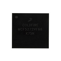
MCF5272VF66 Freescale, MCF5272VF66 Datasheet - Page 336

MCF5272VF66
Manufacturer Part Number
MCF5272VF66
Description
Manufacturer
Freescale
Datasheet
1.MCF5272VF66.pdf
(544 pages)
Specifications of MCF5272VF66
Family Name
MCF5xxx
Device Core
ColdFire
Device Core Size
32b
Frequency (max)
66MHz
Instruction Set Architecture
RISC
Supply Voltage 1 (typ)
3.3V
Operating Temp Range
0C to 70C
Operating Temperature Classification
Commercial
Mounting
Surface Mount
Pin Count
196
Package Type
MA-BGA
Lead Free Status / RoHS Status
Not Compliant
Available stocks
Company
Part Number
Manufacturer
Quantity
Price
Company:
Part Number:
MCF5272VF66
Manufacturer:
HYNIX
Quantity:
19
Company:
Part Number:
MCF5272VF66
Manufacturer:
FREESCAL
Quantity:
885
Company:
Part Number:
MCF5272VF66
Manufacturer:
Freescale Semiconductor
Quantity:
10 000
Part Number:
MCF5272VF66
Manufacturer:
FREESCALE
Quantity:
20 000
Company:
Part Number:
MCF5272VF66J
Manufacturer:
Freescale
Quantity:
256
Company:
Part Number:
MCF5272VF66J
Manufacturer:
Freescale Semiconductor
Quantity:
10 000
Company:
Part Number:
MCF5272VF66R2
Manufacturer:
Freescale Semiconductor
Quantity:
10 000
Company:
Part Number:
MCF5272VF66R2J
Manufacturer:
Freescale Semiconductor
Quantity:
10 000
- Current page: 336 of 544
- Download datasheet (7Mb)
Physical Layer Interface Controller (PLIC)
13.6.4
In this example, port 0 is not used. The port 0 pins are multiplexed with UART0 and in this example, port 0
is used to connect to an external transceiver to provide an RS232 interface. Port 1 is programmed in slave
mode and an external U (or S/T) transceiver is connected to port 1. Port 2 and port 3 are used to connect
up to four external PCM CODECs.
In the above example, Freescale’s MC14LC5480 CODECs and MC145572 U transceiver are shown. The
U transceiver in this example is connected to port 1 and the FSC1 frame sync signal is used exclusively
for synchronizing the data on the U transceiver’s IDL interface. CODECs 1 and 2 are connected to delayed
frame sync 2, DFSC2, which is the output of programmable delay 2. Programmable delay 2 generates a
delayed frame sync with reference to FSC1. Similarly CODECs 3 and 4 are connected to DFSC3 which is
the output of programmable delay 3. Programmable delay 3 generates a delayed frame sync also with
reference to FSC1. The MC14LC5480 CODECs, when in IDL mode, may be programmed using the FSR
pin to select whether the CODEC is receiving and transmitting on the B1 or the B2 time slot (see
MC14LC5480 data sheet for further information).
Figure 13-40
IDL2 10-bit mode with a common frame sync.
13-40
Example 2: ISDN SOHO PBX with Ports 1, 2, and 3
shows the IDL bus timing relationship of the CODECs and U transceiver when in standard
MCF5272
MCF5272 ColdFire
Interface1
Figure 13-39. ISDN SOHO PABX Example
UART0
DFSC2
DFSC3
Dout1
FSC1
DCL1
Din1
®
Integrated Microprocessor User’s Manual, Rev. 3
Tx
Rx
IDL SYNC
DT
DT
IDL CLK
DT
DT
DR
DR
DR
FST
DR
FST
BCLKT
FST
BCLKT
BCLKT
FST
BCLKT
RS232
Transceiver
MC14LC5480
MC14LC5480
MC14LC5480
MC14LC5480
MC145572
CODEC 1
CODEC 2
CODEC 3
CODEC 4
BCLKR
BCLKR
BCLKR
BCLKR
FSR
FSR
FSR
FSR
Vdd
GND
Vdd
Vdd
Vdd
GND
Freescale Semiconductor
Related parts for MCF5272VF66
Image
Part Number
Description
Manufacturer
Datasheet
Request
R
Part Number:
Description:
Mcf5272 Coldfire Integrated Microprocessor User
Manufacturer:
Freescale Semiconductor, Inc
Datasheet:

Part Number:
Description:
MCF5272 Interrupt Service Routine for the Physical Layer Interface Controller
Manufacturer:
Freescale Semiconductor / Motorola
Datasheet:

Part Number:
Description:
TOWER ELEVATOR BOARDS HARDWARE
Manufacturer:
Freescale Semiconductor
Datasheet:

Part Number:
Description:
TOWER SERIAL I/O HARDWARE
Manufacturer:
Freescale Semiconductor
Datasheet:

Part Number:
Description:
LCD MODULE FOR TWR SYSTEM
Manufacturer:
Freescale Semiconductor
Datasheet:

Part Number:
Description:
DAUGHTER LCD WVGA I.MX51
Manufacturer:
Freescale Semiconductor
Datasheet:

Part Number:
Description:
TOWER SYSTEM BOARD MPC5125
Manufacturer:
Freescale Semiconductor
Datasheet:

Part Number:
Description:
KIT EVALUATION I.MX51
Manufacturer:
Freescale Semiconductor
Datasheet:

Part Number:
Description:
KIT DEVELOPMENT WINCE IMX25
Manufacturer:
Freescale Semiconductor
Datasheet:

Part Number:
Description:
TOWER SYSTEM KIT MPC5125
Manufacturer:
Freescale Semiconductor
Datasheet:

Part Number:
Description:
TOWER SYSTEM BOARD K40X256
Manufacturer:
Freescale Semiconductor
Datasheet:

Part Number:
Description:
TOWER SYSTEM KIT K40X256
Manufacturer:
Freescale Semiconductor
Datasheet:

Part Number:
Description:
Microcontrollers (MCU) MX28 PLATFORM DEV KIT
Manufacturer:
Freescale Semiconductor
Datasheet:

Part Number:
Description:
MCU, MPU & DSP Development Tools IAR KickStart Kit for Kinetis K60
Manufacturer:
Freescale Semiconductor
Datasheet:

Part Number:
Description:
24BIT HDMI MX535/08
Manufacturer:
Freescale Semiconductor
Datasheet:


