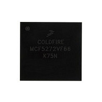
MCF5272VF66 Freescale, MCF5272VF66 Datasheet - Page 395

MCF5272VF66
Manufacturer Part Number
MCF5272VF66
Description
Manufacturer
Freescale
Datasheet
1.MCF5272VF66.pdf
(544 pages)
Specifications of MCF5272VF66
Family Name
MCF5xxx
Device Core
ColdFire
Device Core Size
32b
Frequency (max)
66MHz
Instruction Set Architecture
RISC
Supply Voltage 1 (typ)
3.3V
Operating Temp Range
0C to 70C
Operating Temperature Classification
Commercial
Mounting
Surface Mount
Pin Count
196
Package Type
MA-BGA
Lead Free Status / RoHS Status
Not Compliant
Available stocks
Company
Part Number
Manufacturer
Quantity
Price
Company:
Part Number:
MCF5272VF66
Manufacturer:
HYNIX
Quantity:
19
Company:
Part Number:
MCF5272VF66
Manufacturer:
FREESCAL
Quantity:
885
Company:
Part Number:
MCF5272VF66
Manufacturer:
Freescale Semiconductor
Quantity:
10 000
Part Number:
MCF5272VF66
Manufacturer:
FREESCALE
Quantity:
20 000
Company:
Part Number:
MCF5272VF66J
Manufacturer:
Freescale
Quantity:
256
Company:
Part Number:
MCF5272VF66J
Manufacturer:
Freescale Semiconductor
Quantity:
10 000
Company:
Part Number:
MCF5272VF66R2
Manufacturer:
Freescale Semiconductor
Quantity:
10 000
Company:
Part Number:
MCF5272VF66R2J
Manufacturer:
Freescale Semiconductor
Quantity:
10 000
- Current page: 395 of 544
- Download datasheet (7Mb)
Chapter 17
General Purpose I/O Module
This chapter describes the operation and programming model of the three general-purpose I/O (GPIO)
ports on the MCF5272. It includes details about pin assignment, direction-control, and data registers.
17.1
The MCF5272 provides up to 48 general-purpose I/O signals. The GPIO signal multiplexing is shown in
Table
multifunction GPIO pins default to general purpose inputs and all multifunction pins that are not shared
with a GPIO pin default to high impedance. To avoid indeterminate read values and reduce power
consumption, internal pull-up resistors are active immediately upon reset, and remain active until the
corresponding port direction registers are programmed.
The general-purpose I/O signals are configured as three ports, each having up to 16 signals. These three
general-purpose I/O ports are shared with other signals as follows:
Control registers for each port select the function (GPIO or peripheral pin) assigned to each pin. Pins can
have as many as four functions including GPIO. There is no configuration register for GPIO port C
because its pins are configured by WSEL during device reset.
An additional port, port D, has only a control register which is used to configure the pins that are not
multiplexed with any GPIO signals.
Freescale Semiconductor
17-1. All GPIO pins are individually programmable as inputs or outputs. At reset, all configurable
PA[6:0]
PA7
PA[15:8]
PB[7:0]
PB[15:8]
PC[15:0]
GPIO Signal
Overview
MCF5272 ColdFire
External USB transceiver interface signals
QSPI_CS3 and DOUT3
PLIC TDM ports 0 and 1
UART1 signals and the bus control signal TA
Ethernet controller signals
Data bus signals D[15:0]. These are only available (as GPIO) when the device is
configured for 16-bit data bus mode using the WSEL signal
Table 17-1. GPIO Signal Multiplexing
®
Integrated Microprocessor User’s Manual, Rev. 3
Also Multiplexed on the Same Pins
17-1
Related parts for MCF5272VF66
Image
Part Number
Description
Manufacturer
Datasheet
Request
R
Part Number:
Description:
Mcf5272 Coldfire Integrated Microprocessor User
Manufacturer:
Freescale Semiconductor, Inc
Datasheet:

Part Number:
Description:
MCF5272 Interrupt Service Routine for the Physical Layer Interface Controller
Manufacturer:
Freescale Semiconductor / Motorola
Datasheet:

Part Number:
Description:
TOWER ELEVATOR BOARDS HARDWARE
Manufacturer:
Freescale Semiconductor
Datasheet:

Part Number:
Description:
TOWER SERIAL I/O HARDWARE
Manufacturer:
Freescale Semiconductor
Datasheet:

Part Number:
Description:
LCD MODULE FOR TWR SYSTEM
Manufacturer:
Freescale Semiconductor
Datasheet:

Part Number:
Description:
DAUGHTER LCD WVGA I.MX51
Manufacturer:
Freescale Semiconductor
Datasheet:

Part Number:
Description:
TOWER SYSTEM BOARD MPC5125
Manufacturer:
Freescale Semiconductor
Datasheet:

Part Number:
Description:
KIT EVALUATION I.MX51
Manufacturer:
Freescale Semiconductor
Datasheet:

Part Number:
Description:
KIT DEVELOPMENT WINCE IMX25
Manufacturer:
Freescale Semiconductor
Datasheet:

Part Number:
Description:
TOWER SYSTEM KIT MPC5125
Manufacturer:
Freescale Semiconductor
Datasheet:

Part Number:
Description:
TOWER SYSTEM BOARD K40X256
Manufacturer:
Freescale Semiconductor
Datasheet:

Part Number:
Description:
TOWER SYSTEM KIT K40X256
Manufacturer:
Freescale Semiconductor
Datasheet:

Part Number:
Description:
Microcontrollers (MCU) MX28 PLATFORM DEV KIT
Manufacturer:
Freescale Semiconductor
Datasheet:

Part Number:
Description:
MCU, MPU & DSP Development Tools IAR KickStart Kit for Kinetis K60
Manufacturer:
Freescale Semiconductor
Datasheet:

Part Number:
Description:
24BIT HDMI MX535/08
Manufacturer:
Freescale Semiconductor
Datasheet:


