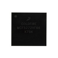
MCF5272VF66 Freescale, MCF5272VF66 Datasheet - Page 288

MCF5272VF66
Manufacturer Part Number
MCF5272VF66
Description
Manufacturer
Freescale
Datasheet
1.MCF5272VF66.pdf
(544 pages)
Specifications of MCF5272VF66
Family Name
MCF5xxx
Device Core
ColdFire
Device Core Size
32b
Frequency (max)
66MHz
Instruction Set Architecture
RISC
Supply Voltage 1 (typ)
3.3V
Operating Temp Range
0C to 70C
Operating Temperature Classification
Commercial
Mounting
Surface Mount
Pin Count
196
Package Type
MA-BGA
Lead Free Status / RoHS Status
Not Compliant
Available stocks
Company
Part Number
Manufacturer
Quantity
Price
Company:
Part Number:
MCF5272VF66
Manufacturer:
HYNIX
Quantity:
19
Company:
Part Number:
MCF5272VF66
Manufacturer:
FREESCAL
Quantity:
885
Company:
Part Number:
MCF5272VF66
Manufacturer:
Freescale Semiconductor
Quantity:
10 000
Part Number:
MCF5272VF66
Manufacturer:
FREESCALE
Quantity:
20 000
Company:
Part Number:
MCF5272VF66J
Manufacturer:
Freescale
Quantity:
256
Company:
Part Number:
MCF5272VF66J
Manufacturer:
Freescale Semiconductor
Quantity:
10 000
Company:
Part Number:
MCF5272VF66R2
Manufacturer:
Freescale Semiconductor
Quantity:
10 000
Company:
Part Number:
MCF5272VF66R2J
Manufacturer:
Freescale Semiconductor
Quantity:
10 000
- Current page: 288 of 544
- Download datasheet (7Mb)
Universal Serial Bus (USB)
12.3.4
The access times for the USB module depend on whether the access is to a register, to an endpoint FIFO
(EPnDR register), or to the configuration RAM.
12.3.4.1
The USB module registers are accessed through the internal S-bus. Each register access takes 3 clock
cycles for reads and writes.
12.3.4.2
The FIFO access time depends on the size, the time between accesses, and whether the previous FIFO
access was for the same endpoint. After a longword access to an endpoint’s FIFO, the next longword in
the FIFO is cached for a quicker access time on the next longword read. This mechanism is reset every
time another endpoint is accessed.
12.3.4.3
The configuration RAM is longword accessible only. Access times for reads from the configuration RAM
are eight clock cycles per access. Clock cycle access times for back-to-back writes to the configuration
RAM are 3-5-5-5-5-5... Access times for writes separated by at least 1 clock cycle are 3-3-3-3-3-3…
12-30
9. Interface #0 Descriptor
10. Endpoint #1 Descriptor
11. Configuration #3 Descriptor
12. Interface #0 Descriptor
13. Endpoint #1 Descriptor
14. Endpoint #2 Descriptor
USB Module Access Times
Registers
Endpoint FIFOs
Configuration RAM
Byte
Word
Long (back to back)
Long (1 clock gap)
Long (2 clock gap)
Long (3+ clock gap)
MCF5272 ColdFire
Access Type
Table 12-19. USB FIFO Access Timing
Table 12-19
®
Integrated Microprocessor User’s Manual, Rev. 3
5
6
8-4-6-6-6-6...
8-3-5-5-5-5...
8-3-4-4-4-4...
8-3-3-3-3-3...
shows the access times for the FIFOs.
Read
4
4
4-6-6-6-6-6...
4-5-5-5-5-5...
4-4-4-4-4-4...
4-4-4-4-4-4...
Write
Freescale Semiconductor
Related parts for MCF5272VF66
Image
Part Number
Description
Manufacturer
Datasheet
Request
R
Part Number:
Description:
Mcf5272 Coldfire Integrated Microprocessor User
Manufacturer:
Freescale Semiconductor, Inc
Datasheet:

Part Number:
Description:
MCF5272 Interrupt Service Routine for the Physical Layer Interface Controller
Manufacturer:
Freescale Semiconductor / Motorola
Datasheet:

Part Number:
Description:
TOWER ELEVATOR BOARDS HARDWARE
Manufacturer:
Freescale Semiconductor
Datasheet:

Part Number:
Description:
TOWER SERIAL I/O HARDWARE
Manufacturer:
Freescale Semiconductor
Datasheet:

Part Number:
Description:
LCD MODULE FOR TWR SYSTEM
Manufacturer:
Freescale Semiconductor
Datasheet:

Part Number:
Description:
DAUGHTER LCD WVGA I.MX51
Manufacturer:
Freescale Semiconductor
Datasheet:

Part Number:
Description:
TOWER SYSTEM BOARD MPC5125
Manufacturer:
Freescale Semiconductor
Datasheet:

Part Number:
Description:
KIT EVALUATION I.MX51
Manufacturer:
Freescale Semiconductor
Datasheet:

Part Number:
Description:
KIT DEVELOPMENT WINCE IMX25
Manufacturer:
Freescale Semiconductor
Datasheet:

Part Number:
Description:
TOWER SYSTEM KIT MPC5125
Manufacturer:
Freescale Semiconductor
Datasheet:

Part Number:
Description:
TOWER SYSTEM BOARD K40X256
Manufacturer:
Freescale Semiconductor
Datasheet:

Part Number:
Description:
TOWER SYSTEM KIT K40X256
Manufacturer:
Freescale Semiconductor
Datasheet:

Part Number:
Description:
Microcontrollers (MCU) MX28 PLATFORM DEV KIT
Manufacturer:
Freescale Semiconductor
Datasheet:

Part Number:
Description:
MCU, MPU & DSP Development Tools IAR KickStart Kit for Kinetis K60
Manufacturer:
Freescale Semiconductor
Datasheet:

Part Number:
Description:
24BIT HDMI MX535/08
Manufacturer:
Freescale Semiconductor
Datasheet:


