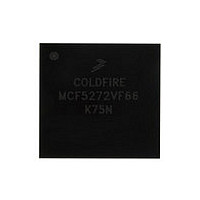
MCF5272VF66 Freescale, MCF5272VF66 Datasheet - Page 157

MCF5272VF66
Manufacturer Part Number
MCF5272VF66
Description
Manufacturer
Freescale
Datasheet
1.MCF5272VF66.pdf
(544 pages)
Specifications of MCF5272VF66
Family Name
MCF5xxx
Device Core
ColdFire
Device Core Size
32b
Frequency (max)
66MHz
Instruction Set Architecture
RISC
Supply Voltage 1 (typ)
3.3V
Operating Temp Range
0C to 70C
Operating Temperature Classification
Commercial
Mounting
Surface Mount
Pin Count
196
Package Type
MA-BGA
Lead Free Status / RoHS Status
Not Compliant
Available stocks
Company
Part Number
Manufacturer
Quantity
Price
Company:
Part Number:
MCF5272VF66
Manufacturer:
HYNIX
Quantity:
19
Company:
Part Number:
MCF5272VF66
Manufacturer:
FREESCAL
Quantity:
885
Company:
Part Number:
MCF5272VF66
Manufacturer:
Freescale Semiconductor
Quantity:
10 000
Part Number:
MCF5272VF66
Manufacturer:
FREESCALE
Quantity:
20 000
Company:
Part Number:
MCF5272VF66J
Manufacturer:
Freescale
Quantity:
256
Company:
Part Number:
MCF5272VF66J
Manufacturer:
Freescale Semiconductor
Quantity:
10 000
Company:
Part Number:
MCF5272VF66R2
Manufacturer:
Freescale Semiconductor
Quantity:
10 000
Company:
Part Number:
MCF5272VF66R2J
Manufacturer:
Freescale Semiconductor
Quantity:
10 000
- Current page: 157 of 544
- Download datasheet (7Mb)
1
2
3
Exception ProcessingPST = 0xC,{PST = 0xB,DD = destination},// stack frame
The PST/DDATA specification for the reset exception is shown below:
Exception ProcessingPST = 0xC,
The initial references at address 0 and 4 are never captured nor displayed since these accesses are treated
as instruction fetches.
For all types of exception processing, the PST = 0xC value is driven at all times, unless the PST output is
needed for one of the optional marker values or for the taken branch indicator (0x5).
Freescale Semiconductor
For JMP and JSR instructions, the optional target instruction address is displayed only for those effective address fields
defining variant addressing modes. This includes the following <ea>x values: (An), (d16,An), (d8,An,Xi), (d8,PC,Xi).
For Move Multiple instructions (MOVEM), the processor automatically generates line-sized transfers if the operand address
reaches a 0-modulo-16 boundary and there are four or more registers to be transferred. For these line-sized transfers, the
operand data is never captured nor displayed, regardless of the CSR value.
The automatic line-sized burst transfers are provided to maximize performance during these sequential memory access
operations.
During normal exception processing, the PST output is driven to a 0xC indicating the exception processing state. The
exception stack write operands, as well as the vector read and target address of the exception handler may also be displayed.
Instruction
wddata.w
wddata.b
wddata.l
rems.l
remu.l
subq.l
subx.l
subi.l
swap
sub.l
sub.l
tst.w
trapf
tst.b
unlk
trap
tst.l
scc
rts
PST = 0x5,{PST = [0x9AB],DD = target}// handler PC
PST = 0x5,{PST = [0x9AB],DD = target} // handler PC
Table 5-22. PST/DDATA Specification for User-Mode Instructions (continued)
Operand Syntax
<ea>y,Dx:Dw
<ea>y,Dx:Dw
{PST = 0xB,DD = destination},// stack frame
{PST = 0xB,DD = source},// vector read
#imm,<ea>x
<ea>y,Rx
Dy,<ea>x
#imm,Dx
MCF5272 ColdFire
<ea>x
<ea>x
<ea>x
<ea>y
<ea>y
<ea>y
Dy,Dx
#imm
Dx
Dx
Ax
PST = 0x1, {PST = 0xB, DD = source operand}
PST = 0x1, {PST = 0xB, DD = source operand}
PST = 0x1, {PST = 0xB, DD = source operand},
PST = 0x5, {PST = [0x9AB], DD = target address}
PST = 0x1
PST = 0x1, {PST = 0xB, DD = source operand}
PST = 0x1, {PST = 0xB, DD = source}, {PST = 0xB, DD = destination}
PST = 0x1
PST = 0x1, {PST = 0xB, DD = source}, {PST = 0xB, DD = destination}
PST = 0x1
PST = 0x1, {PST = 0x8, DD = source operand}
PST = 0x1, {PST = 0xB, DD = source operand}
PST = 0x1, {PST = 0x9, DD = source operand}
PST = 0x1, {PST = 0xB, DD = destination operand}
PST = 0x4, {PST = 0x8, DD = source operand
PST = 0x4, {PST = 0xB, DD = source operand
PST = 0x1
PST = 0x1
PST = 0x1
PST = 0x4, {PST = 0x9, DD = source operand
®
Integrated Microprocessor User’s Manual, Rev. 3
3
PST/DDATA
Debug Support
5-39
Related parts for MCF5272VF66
Image
Part Number
Description
Manufacturer
Datasheet
Request
R
Part Number:
Description:
Mcf5272 Coldfire Integrated Microprocessor User
Manufacturer:
Freescale Semiconductor, Inc
Datasheet:

Part Number:
Description:
MCF5272 Interrupt Service Routine for the Physical Layer Interface Controller
Manufacturer:
Freescale Semiconductor / Motorola
Datasheet:

Part Number:
Description:
TOWER ELEVATOR BOARDS HARDWARE
Manufacturer:
Freescale Semiconductor
Datasheet:

Part Number:
Description:
TOWER SERIAL I/O HARDWARE
Manufacturer:
Freescale Semiconductor
Datasheet:

Part Number:
Description:
LCD MODULE FOR TWR SYSTEM
Manufacturer:
Freescale Semiconductor
Datasheet:

Part Number:
Description:
DAUGHTER LCD WVGA I.MX51
Manufacturer:
Freescale Semiconductor
Datasheet:

Part Number:
Description:
TOWER SYSTEM BOARD MPC5125
Manufacturer:
Freescale Semiconductor
Datasheet:

Part Number:
Description:
KIT EVALUATION I.MX51
Manufacturer:
Freescale Semiconductor
Datasheet:

Part Number:
Description:
KIT DEVELOPMENT WINCE IMX25
Manufacturer:
Freescale Semiconductor
Datasheet:

Part Number:
Description:
TOWER SYSTEM KIT MPC5125
Manufacturer:
Freescale Semiconductor
Datasheet:

Part Number:
Description:
TOWER SYSTEM BOARD K40X256
Manufacturer:
Freescale Semiconductor
Datasheet:

Part Number:
Description:
TOWER SYSTEM KIT K40X256
Manufacturer:
Freescale Semiconductor
Datasheet:

Part Number:
Description:
Microcontrollers (MCU) MX28 PLATFORM DEV KIT
Manufacturer:
Freescale Semiconductor
Datasheet:

Part Number:
Description:
MCU, MPU & DSP Development Tools IAR KickStart Kit for Kinetis K60
Manufacturer:
Freescale Semiconductor
Datasheet:

Part Number:
Description:
24BIT HDMI MX535/08
Manufacturer:
Freescale Semiconductor
Datasheet:


