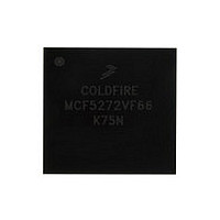
MCF5272VF66 Freescale, MCF5272VF66 Datasheet - Page 311

MCF5272VF66
Manufacturer Part Number
MCF5272VF66
Description
Manufacturer
Freescale
Datasheet
1.MCF5272VF66.pdf
(544 pages)
Specifications of MCF5272VF66
Family Name
MCF5xxx
Device Core
ColdFire
Device Core Size
32b
Frequency (max)
66MHz
Instruction Set Architecture
RISC
Supply Voltage 1 (typ)
3.3V
Operating Temp Range
0C to 70C
Operating Temperature Classification
Commercial
Mounting
Surface Mount
Pin Count
196
Package Type
MA-BGA
Lead Free Status / RoHS Status
Not Compliant
Available stocks
Company
Part Number
Manufacturer
Quantity
Price
Company:
Part Number:
MCF5272VF66
Manufacturer:
HYNIX
Quantity:
19
Company:
Part Number:
MCF5272VF66
Manufacturer:
FREESCAL
Quantity:
885
Company:
Part Number:
MCF5272VF66
Manufacturer:
Freescale Semiconductor
Quantity:
10 000
Part Number:
MCF5272VF66
Manufacturer:
FREESCALE
Quantity:
20 000
Company:
Part Number:
MCF5272VF66J
Manufacturer:
Freescale
Quantity:
256
Company:
Part Number:
MCF5272VF66J
Manufacturer:
Freescale Semiconductor
Quantity:
10 000
Company:
Part Number:
MCF5272VF66R2
Manufacturer:
Freescale Semiconductor
Quantity:
10 000
Company:
Part Number:
MCF5272VF66R2J
Manufacturer:
Freescale Semiconductor
Quantity:
10 000
- Current page: 311 of 544
- Download datasheet (7Mb)
13.5
Any bits in the following registers marked 0 have no function. When the register is a read/write register,
these bits should be cleared.
Some registers are described that control more than one port. In these cases, parentheses indicates to which
port the control bits relate; for example, LM0(0) is the LM0 bit for port 0.
13.5.1
All bits in these registers are read only and are set on hardware or software reset.
The PnB1RRs contain the last four frames of data received on channel B1. (P0B1RR is the B1 channel
data for port 0, P1B1RR is B1 for port 1, and so on.) The data are packed from the least significant byte
(LSB), up to the most significant byte (MSB).
These registers are aligned on longword boundaries from MBAR + 0x300 for P0B1RR to
MBAR + 0x30C for P3B1RR. See
frame and bit alignment within the 32-bit word.
Freescale Semiconductor
Reset
Reset
Field
Field
Addr
R/W
R/W
PLIC Registers
B1 Data Receive Registers (P0B1RR–P3B1RR)
31
15
MBAR + 0x300 (P0B1RR); 0x304 (P1B1RR); 0x308 (P2B1RR); 0x30C (P3B1RR)
MCF5272 ColdFire
Figure 13-13. B1 Receive Data Registers P0B1RR–P3B1RR
1111_1111
1111_1111
Frame 0
Frame 2
Section 13.2.3, “GCI/IDL B- and D-Channel Bit
®
Integrated Microprocessor User’s Manual, Rev. 3
Read Only
Read Only
24
8
23
7
Physical Layer Interface Controller (PLIC)
1111_1111
1111_1111
Frame 1
Frame 3
Alignment,” for the
16
0
13-15
Related parts for MCF5272VF66
Image
Part Number
Description
Manufacturer
Datasheet
Request
R
Part Number:
Description:
Mcf5272 Coldfire Integrated Microprocessor User
Manufacturer:
Freescale Semiconductor, Inc
Datasheet:

Part Number:
Description:
MCF5272 Interrupt Service Routine for the Physical Layer Interface Controller
Manufacturer:
Freescale Semiconductor / Motorola
Datasheet:

Part Number:
Description:
TOWER ELEVATOR BOARDS HARDWARE
Manufacturer:
Freescale Semiconductor
Datasheet:

Part Number:
Description:
TOWER SERIAL I/O HARDWARE
Manufacturer:
Freescale Semiconductor
Datasheet:

Part Number:
Description:
LCD MODULE FOR TWR SYSTEM
Manufacturer:
Freescale Semiconductor
Datasheet:

Part Number:
Description:
DAUGHTER LCD WVGA I.MX51
Manufacturer:
Freescale Semiconductor
Datasheet:

Part Number:
Description:
TOWER SYSTEM BOARD MPC5125
Manufacturer:
Freescale Semiconductor
Datasheet:

Part Number:
Description:
KIT EVALUATION I.MX51
Manufacturer:
Freescale Semiconductor
Datasheet:

Part Number:
Description:
KIT DEVELOPMENT WINCE IMX25
Manufacturer:
Freescale Semiconductor
Datasheet:

Part Number:
Description:
TOWER SYSTEM KIT MPC5125
Manufacturer:
Freescale Semiconductor
Datasheet:

Part Number:
Description:
TOWER SYSTEM BOARD K40X256
Manufacturer:
Freescale Semiconductor
Datasheet:

Part Number:
Description:
TOWER SYSTEM KIT K40X256
Manufacturer:
Freescale Semiconductor
Datasheet:

Part Number:
Description:
Microcontrollers (MCU) MX28 PLATFORM DEV KIT
Manufacturer:
Freescale Semiconductor
Datasheet:

Part Number:
Description:
MCU, MPU & DSP Development Tools IAR KickStart Kit for Kinetis K60
Manufacturer:
Freescale Semiconductor
Datasheet:

Part Number:
Description:
24BIT HDMI MX535/08
Manufacturer:
Freescale Semiconductor
Datasheet:


