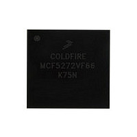
MCF5272VF66 Freescale, MCF5272VF66 Datasheet - Page 191

MCF5272VF66
Manufacturer Part Number
MCF5272VF66
Description
Manufacturer
Freescale
Datasheet
1.MCF5272VF66.pdf
(544 pages)
Specifications of MCF5272VF66
Family Name
MCF5xxx
Device Core
ColdFire
Device Core Size
32b
Frequency (max)
66MHz
Instruction Set Architecture
RISC
Supply Voltage 1 (typ)
3.3V
Operating Temp Range
0C to 70C
Operating Temperature Classification
Commercial
Mounting
Surface Mount
Pin Count
196
Package Type
MA-BGA
Lead Free Status / RoHS Status
Not Compliant
Available stocks
Company
Part Number
Manufacturer
Quantity
Price
Company:
Part Number:
MCF5272VF66
Manufacturer:
HYNIX
Quantity:
19
Company:
Part Number:
MCF5272VF66
Manufacturer:
FREESCAL
Quantity:
885
Company:
Part Number:
MCF5272VF66
Manufacturer:
Freescale Semiconductor
Quantity:
10 000
Part Number:
MCF5272VF66
Manufacturer:
FREESCALE
Quantity:
20 000
Company:
Part Number:
MCF5272VF66J
Manufacturer:
Freescale
Quantity:
256
Company:
Part Number:
MCF5272VF66J
Manufacturer:
Freescale Semiconductor
Quantity:
10 000
Company:
Part Number:
MCF5272VF66R2
Manufacturer:
Freescale Semiconductor
Quantity:
10 000
Company:
Part Number:
MCF5272VF66R2J
Manufacturer:
Freescale Semiconductor
Quantity:
10 000
- Current page: 191 of 544
- Download datasheet (7Mb)
Chapter 9
SDRAM Controller
This chapter describes configuration and operation of the synchronous DRAM controller component of
the SIM including a general description of signals involved in SDRAM operations. It provides interface
information for memory configurations using most common SDRAM devices for both 16- and 32-bit wide
data buses. The chapter concludes with signal timing diagrams.
9.1
The MCF5272 incorporates an SDRAM controller, whose main features are as follows:
9.2
The SDRAM controller provides all required signals for glueless interfacing to a variety of
JEDEC-compliant SDRAM devices. RAS/CAS address multiplexing and the SDRAM pin A10
auto-precharge function is software configurable for different page sizes. To maintain refresh capability
without conflicting with concurrent accesses on the address and data buses, RAS0, CAS0, SDWE,
SDBA[0:1], SDCLKE, A10_PRECHG, and the SDRAM bank selects are dedicated SDRAM signals.
Figure 9-1
Freescale Semiconductor
•
•
•
•
•
•
•
•
•
•
•
Glueless interface to a variety of JEDEC-compliant SDRAM devices.
MCF5272 data bus width of 16 or 32 bits to SDRAM memory array
16- to 256-Mbit device support
Dedicated bank address pins to provide pin out compatibility for different SDRAM sizes with a
single printed circuit board layout
Page size from 256–1024 column address locations
6-1-1-1 timing for burst-read; 3-1-1-1 timing for burst-write accesses (assuming a page hit at 66
MHz)
CAS latencies of 1 and 2
Up to four concurrently activated banks
SDRAM power down and self refresh
Refresh timer prescaler supports system clock down to 5 MHz maintaining a 15.6-µS refresh cycle
Auto initialization of SDRAM
Overview
SDRAM Controller Signals
shows the SDRAM controller signal configuration.
MCF5272 ColdFire
®
Integrated Microprocessor User’s Manual, Rev. 3
9-1
Related parts for MCF5272VF66
Image
Part Number
Description
Manufacturer
Datasheet
Request
R
Part Number:
Description:
Mcf5272 Coldfire Integrated Microprocessor User
Manufacturer:
Freescale Semiconductor, Inc
Datasheet:

Part Number:
Description:
MCF5272 Interrupt Service Routine for the Physical Layer Interface Controller
Manufacturer:
Freescale Semiconductor / Motorola
Datasheet:

Part Number:
Description:
TOWER ELEVATOR BOARDS HARDWARE
Manufacturer:
Freescale Semiconductor
Datasheet:

Part Number:
Description:
TOWER SERIAL I/O HARDWARE
Manufacturer:
Freescale Semiconductor
Datasheet:

Part Number:
Description:
LCD MODULE FOR TWR SYSTEM
Manufacturer:
Freescale Semiconductor
Datasheet:

Part Number:
Description:
DAUGHTER LCD WVGA I.MX51
Manufacturer:
Freescale Semiconductor
Datasheet:

Part Number:
Description:
TOWER SYSTEM BOARD MPC5125
Manufacturer:
Freescale Semiconductor
Datasheet:

Part Number:
Description:
KIT EVALUATION I.MX51
Manufacturer:
Freescale Semiconductor
Datasheet:

Part Number:
Description:
KIT DEVELOPMENT WINCE IMX25
Manufacturer:
Freescale Semiconductor
Datasheet:

Part Number:
Description:
TOWER SYSTEM KIT MPC5125
Manufacturer:
Freescale Semiconductor
Datasheet:

Part Number:
Description:
TOWER SYSTEM BOARD K40X256
Manufacturer:
Freescale Semiconductor
Datasheet:

Part Number:
Description:
TOWER SYSTEM KIT K40X256
Manufacturer:
Freescale Semiconductor
Datasheet:

Part Number:
Description:
Microcontrollers (MCU) MX28 PLATFORM DEV KIT
Manufacturer:
Freescale Semiconductor
Datasheet:

Part Number:
Description:
MCU, MPU & DSP Development Tools IAR KickStart Kit for Kinetis K60
Manufacturer:
Freescale Semiconductor
Datasheet:

Part Number:
Description:
24BIT HDMI MX535/08
Manufacturer:
Freescale Semiconductor
Datasheet:


