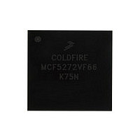
MCF5272VF66 Freescale, MCF5272VF66 Datasheet - Page 295

MCF5272VF66
Manufacturer Part Number
MCF5272VF66
Description
Manufacturer
Freescale
Datasheet
1.MCF5272VF66.pdf
(544 pages)
Specifications of MCF5272VF66
Family Name
MCF5xxx
Device Core
ColdFire
Device Core Size
32b
Frequency (max)
66MHz
Instruction Set Architecture
RISC
Supply Voltage 1 (typ)
3.3V
Operating Temp Range
0C to 70C
Operating Temperature Classification
Commercial
Mounting
Surface Mount
Pin Count
196
Package Type
MA-BGA
Lead Free Status / RoHS Status
Not Compliant
Available stocks
Company
Part Number
Manufacturer
Quantity
Price
Company:
Part Number:
MCF5272VF66
Manufacturer:
HYNIX
Quantity:
19
Company:
Part Number:
MCF5272VF66
Manufacturer:
FREESCAL
Quantity:
885
Company:
Part Number:
MCF5272VF66
Manufacturer:
Freescale Semiconductor
Quantity:
10 000
Part Number:
MCF5272VF66
Manufacturer:
FREESCALE
Quantity:
20 000
Company:
Part Number:
MCF5272VF66J
Manufacturer:
Freescale
Quantity:
256
Company:
Part Number:
MCF5272VF66J
Manufacturer:
Freescale Semiconductor
Quantity:
10 000
Company:
Part Number:
MCF5272VF66R2
Manufacturer:
Freescale Semiconductor
Quantity:
10 000
Company:
Part Number:
MCF5272VF66R2J
Manufacturer:
Freescale Semiconductor
Quantity:
10 000
- Current page: 295 of 544
- Download datasheet (7Mb)
12.5.3
Figure 12-25
Freescale Semiconductor
•
•
•
•
Bypass capacitors should be connected between the Vdd and GND pairs with minimal trace length.
These capacitors help supply the instantaneous currents of the digital circuitry, in addition to
decoupling the noise that may be generated by other sections of the device or other circuitry on the
power supply.
Use short, wide, low inductance traces to connect all of the GND pins together and, with a single
trace, connect all of the GND pins to the power supply ground. This helps to reduce voltage spikes
in the ground circuit caused by high-speed digital current spikes. Suppressing these voltage spikes
on the integrated circuit is the reason for multiple GND leads. A PCB with a ground plane
connecting all of the digital and analog GND pins together is the optimal ground configuration,
producing the lowest resistance and inductance in the ground circuit.
Use short, wide, low inductance traces to connect all of the Vdd power supply pins together and,
with a single trace, connect all of the Vdd pins to the 3.3V power supply. Connecting all of the
digital and analog Vdd pins to the power plane would be the optimal power distribution method for
a multi-layer PCB with a power plane.
The 48-MHz oscillator must be located as close as possible to the chip package. This is required to
minimize parasitic capacitance between crystal traces and ground.
Recommended USB Protection Circuit
shows the recommended external ESD protection circuit for the USB.
D +
D –
MCF5272 ColdFire
+3.3V
22pF
+3.3V
2 x MMBD301LT1
Figure 12-25. USB Protection Circuit
Schottky Diode
®
Integrated Microprocessor User’s Manual, Rev. 3
22pF
33
33
BZX84C3V3LT1
Zener Diode
1.5K
0.1μF
330
USB Port
1
2
3
4
Universal Serial Bus (USB)
12-37
Related parts for MCF5272VF66
Image
Part Number
Description
Manufacturer
Datasheet
Request
R
Part Number:
Description:
Mcf5272 Coldfire Integrated Microprocessor User
Manufacturer:
Freescale Semiconductor, Inc
Datasheet:

Part Number:
Description:
MCF5272 Interrupt Service Routine for the Physical Layer Interface Controller
Manufacturer:
Freescale Semiconductor / Motorola
Datasheet:

Part Number:
Description:
TOWER ELEVATOR BOARDS HARDWARE
Manufacturer:
Freescale Semiconductor
Datasheet:

Part Number:
Description:
TOWER SERIAL I/O HARDWARE
Manufacturer:
Freescale Semiconductor
Datasheet:

Part Number:
Description:
LCD MODULE FOR TWR SYSTEM
Manufacturer:
Freescale Semiconductor
Datasheet:

Part Number:
Description:
DAUGHTER LCD WVGA I.MX51
Manufacturer:
Freescale Semiconductor
Datasheet:

Part Number:
Description:
TOWER SYSTEM BOARD MPC5125
Manufacturer:
Freescale Semiconductor
Datasheet:

Part Number:
Description:
KIT EVALUATION I.MX51
Manufacturer:
Freescale Semiconductor
Datasheet:

Part Number:
Description:
KIT DEVELOPMENT WINCE IMX25
Manufacturer:
Freescale Semiconductor
Datasheet:

Part Number:
Description:
TOWER SYSTEM KIT MPC5125
Manufacturer:
Freescale Semiconductor
Datasheet:

Part Number:
Description:
TOWER SYSTEM BOARD K40X256
Manufacturer:
Freescale Semiconductor
Datasheet:

Part Number:
Description:
TOWER SYSTEM KIT K40X256
Manufacturer:
Freescale Semiconductor
Datasheet:

Part Number:
Description:
Microcontrollers (MCU) MX28 PLATFORM DEV KIT
Manufacturer:
Freescale Semiconductor
Datasheet:

Part Number:
Description:
MCU, MPU & DSP Development Tools IAR KickStart Kit for Kinetis K60
Manufacturer:
Freescale Semiconductor
Datasheet:

Part Number:
Description:
24BIT HDMI MX535/08
Manufacturer:
Freescale Semiconductor
Datasheet:


