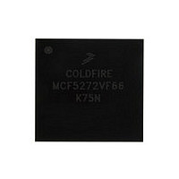
MCF5272VF66 Freescale, MCF5272VF66 Datasheet - Page 186

MCF5272VF66
Manufacturer Part Number
MCF5272VF66
Description
Manufacturer
Freescale
Datasheet
1.MCF5272VF66.pdf
(544 pages)
Specifications of MCF5272VF66
Family Name
MCF5xxx
Device Core
ColdFire
Device Core Size
32b
Frequency (max)
66MHz
Instruction Set Architecture
RISC
Supply Voltage 1 (typ)
3.3V
Operating Temp Range
0C to 70C
Operating Temperature Classification
Commercial
Mounting
Surface Mount
Pin Count
196
Package Type
MA-BGA
Lead Free Status / RoHS Status
Not Compliant
Available stocks
Company
Part Number
Manufacturer
Quantity
Price
Company:
Part Number:
MCF5272VF66
Manufacturer:
HYNIX
Quantity:
19
Company:
Part Number:
MCF5272VF66
Manufacturer:
FREESCAL
Quantity:
885
Company:
Part Number:
MCF5272VF66
Manufacturer:
Freescale Semiconductor
Quantity:
10 000
Part Number:
MCF5272VF66
Manufacturer:
FREESCALE
Quantity:
20 000
Company:
Part Number:
MCF5272VF66J
Manufacturer:
Freescale
Quantity:
256
Company:
Part Number:
MCF5272VF66J
Manufacturer:
Freescale Semiconductor
Quantity:
10 000
Company:
Part Number:
MCF5272VF66R2
Manufacturer:
Freescale Semiconductor
Quantity:
10 000
Company:
Part Number:
MCF5272VF66R2J
Manufacturer:
Freescale Semiconductor
Quantity:
10 000
- Current page: 186 of 544
- Download datasheet (7Mb)
Chip Select Module
8.1.3
CS0 is enabled after reset and is used to access boot ROM. The memory port width of CS0 is defined by
the state of QSPI_CLK/BUSW1 and QSPI_CS0/BUSW0. These two bits should be configured to define
the width of the boot ROM connected to CS0, as described in
Configuration
8.2
Each chip select is controlled through two 32-bit registers. The chip select base registers (CSBR0–CSBR7)
are used to enable the chip select and to configure the base address, port size, bus interface type, and
address space. The chip select option registers (CSOR0–CSOR7) are used to configure the address mask,
additional setup/hold, extended burst capability, wait states, and read/write access.
8-2
Chip Select Registers
Boot CS0 Operation
Pins.”
1
+ 0x04C CSOR1 CS option register 1
+ 0x05C CSOR3 CS option register 3
+ 0x06C CSOR5 CS option register 5
+ 0x07C CSOR7 CS option register 7
+ 0x040
+ 0x044
+ 0x048
+ 0x050
+ 0x054
+ 0x058
+ 0x060
+ 0x064
+ 0x068
+ 0x070
+ 0x074
+ 0x078
Offset
The nibble shown as x resets as 00xx, where the undefined bits represent the
BW field. QSPI_CS0/BUSW0 and QSPI_CLK/BUSW1 program the bus width
for CS0 at reset
MCF5272 ColdFire
CSOR0 CS option register 0
CSOR2 CS option register 2
CSOR4 CS option register 4
CSOR6 CS option register 6
CSBR0 CS base register 0
CSBR1 CS base register 1
CSBR2 CS base register 2
CSBR3 CS base register 3
CSBR4 CS base register 4
CSBR5 CS base register 5
CSBR6 CS base register 6
CSBR7 CS base register 7
Name
Table 8-1. CSCR and CSOR Values after Reset
®
Integrated Microprocessor User’s Manual, Rev. 3
Chip Select Register
Section 19.18, “Operating Mode
0x0000_0x01
0xFFFF_F078
0xFFFF_F078
0xFFFF_F078
0xFFFF_F078
0xFFFF_F078
0xFFFF_F078
0xFFFF_F078
0xFFFF_F078
0x0000_1300
0x0000_2300
0x0000_3300
0x0000_4300
0x0000_5300
0x0000_6300
0x0000_7700
Reset
1
Freescale Semiconductor
Related parts for MCF5272VF66
Image
Part Number
Description
Manufacturer
Datasheet
Request
R
Part Number:
Description:
Mcf5272 Coldfire Integrated Microprocessor User
Manufacturer:
Freescale Semiconductor, Inc
Datasheet:

Part Number:
Description:
MCF5272 Interrupt Service Routine for the Physical Layer Interface Controller
Manufacturer:
Freescale Semiconductor / Motorola
Datasheet:

Part Number:
Description:
TOWER ELEVATOR BOARDS HARDWARE
Manufacturer:
Freescale Semiconductor
Datasheet:

Part Number:
Description:
TOWER SERIAL I/O HARDWARE
Manufacturer:
Freescale Semiconductor
Datasheet:

Part Number:
Description:
LCD MODULE FOR TWR SYSTEM
Manufacturer:
Freescale Semiconductor
Datasheet:

Part Number:
Description:
DAUGHTER LCD WVGA I.MX51
Manufacturer:
Freescale Semiconductor
Datasheet:

Part Number:
Description:
TOWER SYSTEM BOARD MPC5125
Manufacturer:
Freescale Semiconductor
Datasheet:

Part Number:
Description:
KIT EVALUATION I.MX51
Manufacturer:
Freescale Semiconductor
Datasheet:

Part Number:
Description:
KIT DEVELOPMENT WINCE IMX25
Manufacturer:
Freescale Semiconductor
Datasheet:

Part Number:
Description:
TOWER SYSTEM KIT MPC5125
Manufacturer:
Freescale Semiconductor
Datasheet:

Part Number:
Description:
TOWER SYSTEM BOARD K40X256
Manufacturer:
Freescale Semiconductor
Datasheet:

Part Number:
Description:
TOWER SYSTEM KIT K40X256
Manufacturer:
Freescale Semiconductor
Datasheet:

Part Number:
Description:
Microcontrollers (MCU) MX28 PLATFORM DEV KIT
Manufacturer:
Freescale Semiconductor
Datasheet:

Part Number:
Description:
MCU, MPU & DSP Development Tools IAR KickStart Kit for Kinetis K60
Manufacturer:
Freescale Semiconductor
Datasheet:

Part Number:
Description:
24BIT HDMI MX535/08
Manufacturer:
Freescale Semiconductor
Datasheet:


