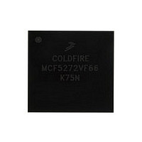
MCF5272VF66 Freescale, MCF5272VF66 Datasheet - Page 140

MCF5272VF66
Manufacturer Part Number
MCF5272VF66
Description
Manufacturer
Freescale
Datasheet
1.MCF5272VF66.pdf
(544 pages)
Specifications of MCF5272VF66
Family Name
MCF5xxx
Device Core
ColdFire
Device Core Size
32b
Frequency (max)
66MHz
Instruction Set Architecture
RISC
Supply Voltage 1 (typ)
3.3V
Operating Temp Range
0C to 70C
Operating Temperature Classification
Commercial
Mounting
Surface Mount
Pin Count
196
Package Type
MA-BGA
Lead Free Status / RoHS Status
Not Compliant
Available stocks
Company
Part Number
Manufacturer
Quantity
Price
Company:
Part Number:
MCF5272VF66
Manufacturer:
HYNIX
Quantity:
19
Company:
Part Number:
MCF5272VF66
Manufacturer:
FREESCAL
Quantity:
885
Company:
Part Number:
MCF5272VF66
Manufacturer:
Freescale Semiconductor
Quantity:
10 000
Part Number:
MCF5272VF66
Manufacturer:
FREESCALE
Quantity:
20 000
Company:
Part Number:
MCF5272VF66J
Manufacturer:
Freescale
Quantity:
256
Company:
Part Number:
MCF5272VF66J
Manufacturer:
Freescale Semiconductor
Quantity:
10 000
Company:
Part Number:
MCF5272VF66R2
Manufacturer:
Freescale Semiconductor
Quantity:
10 000
Company:
Part Number:
MCF5272VF66R2J
Manufacturer:
Freescale Semiconductor
Quantity:
10 000
- Current page: 140 of 544
- Download datasheet (7Mb)
Debug Support
5.5.3.3
The following sections describe the commands summarized in
Freescale reserves unassigned command opcodes for future expansion. Unused command formats in any
revision level perform a
5.5.3.3.1
Read the selected address or data register and return the 32-bit result. A bus error response is returned if
the CPU core is not halted.
Command/Result Formats:
Command Sequence:
Operand Data:
Result Data:
5-22
•
•
•
Command
Result
In cycle 3, the development system supplies the low-order 16 address bits. The debug module
always returns a not-ready response.
At the completion of cycle 3, the debug module initiates a memory read operation. Any serial
transfers that begin during a memory access return a not-ready response.
Results are returned in the two serial transfer cycles after the memory access completes. For any
command performing a byte-sized memory read operation, the upper 8 bits of the response data are
undefined and the referenced data is returned in the lower 8 bits. The next command’s opcode is
sent to the debug module during the final transfer. If a memory or register access is terminated with
a bus error, the error status (S = 1, DATA = 0x0001) is returned instead of result data.
Command Set Descriptions
The BDM status bit (S) is 0 for normally completed commands; S = 1 for
illegal commands, not-ready responses, and transfers with bus-errors.
Section 5.5.2, “BDM Serial
Read A/D Register (
15
MCF5272 ColdFire
None
The contents of the selected register are returned as a longword value,
most-significant word first.
0x2
NOP
Figure 5-18. RAREG
Figure 5-17. RAREG
and return an illegal command response.
RAREG/RDREG
12
???
RAREG
®
11
Integrated Microprocessor User’s Manual, Rev. 3
Interface,” describes the receive packet format.
/
0x1
RDREG
/
RDREG Command Sequence
NOTE
/
RDREG Command Format
MS RESULT
)
BERR
XXX
XXX
D[31:16]
8
D[15:0]
7
Table
LS RESULT
"NOT READY"
NEXT CMD
NEXT CMD
0x8
5-17.
4
A/D
3
Freescale Semiconductor
2
Register
0
Related parts for MCF5272VF66
Image
Part Number
Description
Manufacturer
Datasheet
Request
R
Part Number:
Description:
Mcf5272 Coldfire Integrated Microprocessor User
Manufacturer:
Freescale Semiconductor, Inc
Datasheet:

Part Number:
Description:
MCF5272 Interrupt Service Routine for the Physical Layer Interface Controller
Manufacturer:
Freescale Semiconductor / Motorola
Datasheet:

Part Number:
Description:
TOWER ELEVATOR BOARDS HARDWARE
Manufacturer:
Freescale Semiconductor
Datasheet:

Part Number:
Description:
TOWER SERIAL I/O HARDWARE
Manufacturer:
Freescale Semiconductor
Datasheet:

Part Number:
Description:
LCD MODULE FOR TWR SYSTEM
Manufacturer:
Freescale Semiconductor
Datasheet:

Part Number:
Description:
DAUGHTER LCD WVGA I.MX51
Manufacturer:
Freescale Semiconductor
Datasheet:

Part Number:
Description:
TOWER SYSTEM BOARD MPC5125
Manufacturer:
Freescale Semiconductor
Datasheet:

Part Number:
Description:
KIT EVALUATION I.MX51
Manufacturer:
Freescale Semiconductor
Datasheet:

Part Number:
Description:
KIT DEVELOPMENT WINCE IMX25
Manufacturer:
Freescale Semiconductor
Datasheet:

Part Number:
Description:
TOWER SYSTEM KIT MPC5125
Manufacturer:
Freescale Semiconductor
Datasheet:

Part Number:
Description:
TOWER SYSTEM BOARD K40X256
Manufacturer:
Freescale Semiconductor
Datasheet:

Part Number:
Description:
TOWER SYSTEM KIT K40X256
Manufacturer:
Freescale Semiconductor
Datasheet:

Part Number:
Description:
Microcontrollers (MCU) MX28 PLATFORM DEV KIT
Manufacturer:
Freescale Semiconductor
Datasheet:

Part Number:
Description:
MCU, MPU & DSP Development Tools IAR KickStart Kit for Kinetis K60
Manufacturer:
Freescale Semiconductor
Datasheet:

Part Number:
Description:
24BIT HDMI MX535/08
Manufacturer:
Freescale Semiconductor
Datasheet:


