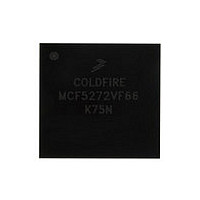
MCF5272VF66 Freescale, MCF5272VF66 Datasheet - Page 433

MCF5272VF66
Manufacturer Part Number
MCF5272VF66
Description
Manufacturer
Freescale
Datasheet
1.MCF5272VF66.pdf
(544 pages)
Specifications of MCF5272VF66
Family Name
MCF5xxx
Device Core
ColdFire
Device Core Size
32b
Frequency (max)
66MHz
Instruction Set Architecture
RISC
Supply Voltage 1 (typ)
3.3V
Operating Temp Range
0C to 70C
Operating Temperature Classification
Commercial
Mounting
Surface Mount
Pin Count
196
Package Type
MA-BGA
Lead Free Status / RoHS Status
Not Compliant
Available stocks
Company
Part Number
Manufacturer
Quantity
Price
Company:
Part Number:
MCF5272VF66
Manufacturer:
HYNIX
Quantity:
19
Company:
Part Number:
MCF5272VF66
Manufacturer:
FREESCAL
Quantity:
885
Company:
Part Number:
MCF5272VF66
Manufacturer:
Freescale Semiconductor
Quantity:
10 000
Part Number:
MCF5272VF66
Manufacturer:
FREESCALE
Quantity:
20 000
Company:
Part Number:
MCF5272VF66J
Manufacturer:
Freescale
Quantity:
256
Company:
Part Number:
MCF5272VF66J
Manufacturer:
Freescale Semiconductor
Quantity:
10 000
Company:
Part Number:
MCF5272VF66R2
Manufacturer:
Freescale Semiconductor
Quantity:
10 000
Company:
Part Number:
MCF5272VF66R2J
Manufacturer:
Freescale Semiconductor
Quantity:
10 000
- Current page: 433 of 544
- Download datasheet (7Mb)
19.6.12 SDRAM Bank Selects (SDBA[1:0])
These outputs are the SDRAM bank select signals.
19.6.13 SDRAM Row Address 10 (A10)/A10 Precharge (A10_PRECHG)
This output is the SDRAM row address 10 and the precharge strobe.
19.7
This section describes clock and reset signals in the CPU.
19.7.1
RSTI is the primary reset input to the device. Asserting RSTI immediately resets the CPU and peripherals.
However, the reset of the SDRAM controller and hence SDRAM contents depend on DRESETEN.
Asserting RSTI also causes RSTO to be asserted for 32K CPU clock cycles.
19.7.2
DRESETEN is asserted to indicate that the SDRAM controller is to be reset whenever RSTI asserts. If
DRESETEN is high, RSTI does not affect the SDRAM controller, which continues to refresh external
memory. This is useful for debug situations where a reset of the device is required without losing data
located in SDRAM. DRESETEN is normally tied high or low depending on system requirements. It should
never be tied to RSTI or RSTO.
19.7.3
CLKIN should be connected to an external clock oscillator. The CLKIN input frequency can range from
DC to 66 MHz. The frequency input to this signal must be greater than twice the frequency applied at E_Tx
CLK. The clock frequency applied to CLKIN must exceed 24 MHz when the system uses a USB
peripheral.
19.7.4
Reset output (RSTO) is driven low for 128 CPU clocks when the soft reset bit of the system configuration
register (SCR[SOFTRST]) is set. It is driven low for 32K CPU clocks when the software watchdog timer
times out or when a low input level is applied to RSTI.
19.8
The six interrupt request inputs (INT[6:1]) can generate separate, maskable interrupts on negative edge
(high to low) or positive edge (low to high) transitions. In addition to the triggering edge being
programmable, the priority can also be programmed. Each interrupt input has a separate programmable
interrupt level.
Freescale Semiconductor
CPU Clock and Reset Signals
Interrupt Request Inputs (INT[6:1])
RSTI
DRESETEN
CPU External Clock (CLKIN)
Reset Output (RSTO)
MCF5272 ColdFire
®
Integrated Microprocessor User’s Manual, Rev. 3
Signal Descriptions
19-23
Related parts for MCF5272VF66
Image
Part Number
Description
Manufacturer
Datasheet
Request
R
Part Number:
Description:
Mcf5272 Coldfire Integrated Microprocessor User
Manufacturer:
Freescale Semiconductor, Inc
Datasheet:

Part Number:
Description:
MCF5272 Interrupt Service Routine for the Physical Layer Interface Controller
Manufacturer:
Freescale Semiconductor / Motorola
Datasheet:

Part Number:
Description:
TOWER ELEVATOR BOARDS HARDWARE
Manufacturer:
Freescale Semiconductor
Datasheet:

Part Number:
Description:
TOWER SERIAL I/O HARDWARE
Manufacturer:
Freescale Semiconductor
Datasheet:

Part Number:
Description:
LCD MODULE FOR TWR SYSTEM
Manufacturer:
Freescale Semiconductor
Datasheet:

Part Number:
Description:
DAUGHTER LCD WVGA I.MX51
Manufacturer:
Freescale Semiconductor
Datasheet:

Part Number:
Description:
TOWER SYSTEM BOARD MPC5125
Manufacturer:
Freescale Semiconductor
Datasheet:

Part Number:
Description:
KIT EVALUATION I.MX51
Manufacturer:
Freescale Semiconductor
Datasheet:

Part Number:
Description:
KIT DEVELOPMENT WINCE IMX25
Manufacturer:
Freescale Semiconductor
Datasheet:

Part Number:
Description:
TOWER SYSTEM KIT MPC5125
Manufacturer:
Freescale Semiconductor
Datasheet:

Part Number:
Description:
TOWER SYSTEM BOARD K40X256
Manufacturer:
Freescale Semiconductor
Datasheet:

Part Number:
Description:
TOWER SYSTEM KIT K40X256
Manufacturer:
Freescale Semiconductor
Datasheet:

Part Number:
Description:
Microcontrollers (MCU) MX28 PLATFORM DEV KIT
Manufacturer:
Freescale Semiconductor
Datasheet:

Part Number:
Description:
MCU, MPU & DSP Development Tools IAR KickStart Kit for Kinetis K60
Manufacturer:
Freescale Semiconductor
Datasheet:

Part Number:
Description:
24BIT HDMI MX535/08
Manufacturer:
Freescale Semiconductor
Datasheet:


