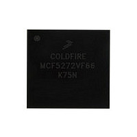
MCF5272VF66 Freescale, MCF5272VF66 Datasheet - Page 345

MCF5272VF66
Manufacturer Part Number
MCF5272VF66
Description
Manufacturer
Freescale
Datasheet
1.MCF5272VF66.pdf
(544 pages)
Specifications of MCF5272VF66
Family Name
MCF5xxx
Device Core
ColdFire
Device Core Size
32b
Frequency (max)
66MHz
Instruction Set Architecture
RISC
Supply Voltage 1 (typ)
3.3V
Operating Temp Range
0C to 70C
Operating Temperature Classification
Commercial
Mounting
Surface Mount
Pin Count
196
Package Type
MA-BGA
Lead Free Status / RoHS Status
Not Compliant
Available stocks
Company
Part Number
Manufacturer
Quantity
Price
Company:
Part Number:
MCF5272VF66
Manufacturer:
HYNIX
Quantity:
19
Company:
Part Number:
MCF5272VF66
Manufacturer:
FREESCAL
Quantity:
885
Company:
Part Number:
MCF5272VF66
Manufacturer:
Freescale Semiconductor
Quantity:
10 000
Part Number:
MCF5272VF66
Manufacturer:
FREESCALE
Quantity:
20 000
Company:
Part Number:
MCF5272VF66J
Manufacturer:
Freescale
Quantity:
256
Company:
Part Number:
MCF5272VF66J
Manufacturer:
Freescale Semiconductor
Quantity:
10 000
Company:
Part Number:
MCF5272VF66R2
Manufacturer:
Freescale Semiconductor
Quantity:
10 000
Company:
Part Number:
MCF5272VF66R2J
Manufacturer:
Freescale Semiconductor
Quantity:
10 000
- Current page: 345 of 544
- Download datasheet (7Mb)
14.4.3
The QSPI supports programmable delays for the QSPI_CS signals before and after a transfer. The time
between QSPI_CS assertion and the leading QSPI_CLK edge, and the time between the end of one transfer
and the beginning of the next, are both independently programmable.
The chip select to clock delay enable (DSCK) bit in command RAM, QCR[DSCK], enables the
programmable delay period from QSPI_CS assertion until the leading edge of QSPI_CLK. QDLYR[QCD]
determines the period of delay before the leading edge of QSPI_CLK. The following expression
determines the actual delay before the QSPI_CLK leading edge:
QSPI_CS-to-QSPI_CLK delay = QCD/CLKIN frequency
QCD has a range of 1–127.
When QCD or DSCK equals zero, the standard delay of one-half the QSPI_CLK period is used.
The delay after transmit enable (DT) bit in command RAM enables the programmable delay period from
the negation of the QSPI_CS signals until the start of the next transfer. The delay after transfer can be used
to provide a peripheral deselect interval. A delay can also be inserted between consecutive transfers to
allow serial A/D converters to complete conversion. There are two transfer delay options: the user can
choose to delay a standard period after serial transfer is complete or can specify a delay period. Writing a
value to QDLYR[DTL] specifies a delay period. The DT bit in command RAM determines whether the
standard delay period (DT = 0) or the specified delay period (DT = 1) is used. The following expression
is used to calculate the delay:
Delay after transfer = 32 × QDLYR[DTL] /CLKIN frequency (DT = 1)
where QDLYR[DTL] has a range of 1–255.
A zero value for DTL causes a delay-after-transfer value of 8192/CLKIN frequency.
Standard delay after transfer = 17/CLKIN frequency (DT = 0)
Receiving devices need at least the standard delay (DT=0) between successive transfers for long data
streams because the QSPI module requires time to load a transmit RAM entry for transfer. If CLKIN is
operating at a slower rate, the delay between transfers must be increased proportionately.
Freescale Semiconductor
Transfer Delays
Table 14-2. QSPI_CLK Frequency as Function of CPU Clock and Baud Rate
QMR [BAUD]
255
16
32
2
4
8
MCF5272 ColdFire
®
66 MHz
Integrated Microprocessor User’s Manual, Rev. 3
16,500,000
8,250,000
4,125,000
2,062,500
1,031,250
129,412
48 MHz
12,000,000
6,000,000
3,000,000
1,500,000
750,000
94,118
CPU Clock
Queued Serial Peripheral Interface (QSPI) Module
33 MHz
8,250,000
4,125,000
2,062,500
1,031,250
515,625
64,706
20 MHz
5,000,000
2,500,000
1,250,000
625,000
312,500
39,216
14-7
Related parts for MCF5272VF66
Image
Part Number
Description
Manufacturer
Datasheet
Request
R
Part Number:
Description:
Mcf5272 Coldfire Integrated Microprocessor User
Manufacturer:
Freescale Semiconductor, Inc
Datasheet:

Part Number:
Description:
MCF5272 Interrupt Service Routine for the Physical Layer Interface Controller
Manufacturer:
Freescale Semiconductor / Motorola
Datasheet:

Part Number:
Description:
TOWER ELEVATOR BOARDS HARDWARE
Manufacturer:
Freescale Semiconductor
Datasheet:

Part Number:
Description:
TOWER SERIAL I/O HARDWARE
Manufacturer:
Freescale Semiconductor
Datasheet:

Part Number:
Description:
LCD MODULE FOR TWR SYSTEM
Manufacturer:
Freescale Semiconductor
Datasheet:

Part Number:
Description:
DAUGHTER LCD WVGA I.MX51
Manufacturer:
Freescale Semiconductor
Datasheet:

Part Number:
Description:
TOWER SYSTEM BOARD MPC5125
Manufacturer:
Freescale Semiconductor
Datasheet:

Part Number:
Description:
KIT EVALUATION I.MX51
Manufacturer:
Freescale Semiconductor
Datasheet:

Part Number:
Description:
KIT DEVELOPMENT WINCE IMX25
Manufacturer:
Freescale Semiconductor
Datasheet:

Part Number:
Description:
TOWER SYSTEM KIT MPC5125
Manufacturer:
Freescale Semiconductor
Datasheet:

Part Number:
Description:
TOWER SYSTEM BOARD K40X256
Manufacturer:
Freescale Semiconductor
Datasheet:

Part Number:
Description:
TOWER SYSTEM KIT K40X256
Manufacturer:
Freescale Semiconductor
Datasheet:

Part Number:
Description:
Microcontrollers (MCU) MX28 PLATFORM DEV KIT
Manufacturer:
Freescale Semiconductor
Datasheet:

Part Number:
Description:
MCU, MPU & DSP Development Tools IAR KickStart Kit for Kinetis K60
Manufacturer:
Freescale Semiconductor
Datasheet:

Part Number:
Description:
24BIT HDMI MX535/08
Manufacturer:
Freescale Semiconductor
Datasheet:


