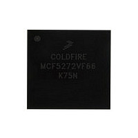
MCF5272VF66 Freescale, MCF5272VF66 Datasheet - Page 355

MCF5272VF66
Manufacturer Part Number
MCF5272VF66
Description
Manufacturer
Freescale
Datasheet
1.MCF5272VF66.pdf
(544 pages)
Specifications of MCF5272VF66
Family Name
MCF5xxx
Device Core
ColdFire
Device Core Size
32b
Frequency (max)
66MHz
Instruction Set Architecture
RISC
Supply Voltage 1 (typ)
3.3V
Operating Temp Range
0C to 70C
Operating Temperature Classification
Commercial
Mounting
Surface Mount
Pin Count
196
Package Type
MA-BGA
Lead Free Status / RoHS Status
Not Compliant
Available stocks
Company
Part Number
Manufacturer
Quantity
Price
Company:
Part Number:
MCF5272VF66
Manufacturer:
HYNIX
Quantity:
19
Company:
Part Number:
MCF5272VF66
Manufacturer:
FREESCAL
Quantity:
885
Company:
Part Number:
MCF5272VF66
Manufacturer:
Freescale Semiconductor
Quantity:
10 000
Part Number:
MCF5272VF66
Manufacturer:
FREESCALE
Quantity:
20 000
Company:
Part Number:
MCF5272VF66J
Manufacturer:
Freescale
Quantity:
256
Company:
Part Number:
MCF5272VF66J
Manufacturer:
Freescale Semiconductor
Quantity:
10 000
Company:
Part Number:
MCF5272VF66R2
Manufacturer:
Freescale Semiconductor
Quantity:
10 000
Company:
Part Number:
MCF5272VF66R2J
Manufacturer:
Freescale Semiconductor
Quantity:
10 000
- Current page: 355 of 544
- Download datasheet (7Mb)
Chapter 15
Timer Module
This chapter describes configuration and operation of the four general-purpose timer modules, timer 0, 1,
2 and 3.
15.1
The timer module has four identical general-purpose 16-bit timers and a software watchdog timer,
described in
Each general-purpose timer consists of a timer mode register (TMRn), a timer capture register (TCAPn),
a 16-bit timer counter (TCNn), a timer reference register (TRRn), and a timer event register (TERn). The
TMRs contain the prescaler value programmed by the user. The four timer units have the following
features:
15.2
The timer units consist of four identical, independent 16-bit timers, timers 0–3. For timers 0 and 1, the
clock input to the prescaler is selected from the main clock (divided by 1 or 16) or from the corresponding
timer input (TIN0 or TIN1) pin. For timers 2 and 3, the clock input to the prescaler can be selected only
from the main clock (divided by 1 or 16). TIN is internally synchronized to the internal clock, with a
synchronization delay between two and three main clocks. The clock input source is selected by the CLK
bits of the corresponding timer mode register (TMR0–TMR3). The prescaler is programmed to divide the
clock input by values from 1 to 256. The output of the prescaler is used as an input to the 16-bit counter.
The maximum timer resolution is one system clock cycle (15 nS at 66 MHz). The maximum period (the
reference value is all ones) is 268,435,456 cycles = 2
The timer can be configured to count until a reference is reached at which point it can either start a new
time count immediately or continue to run. The free run/restart bit, TMRn[FRR], selects each mode. Upon
reaching the reference value, the TER0 or TER1 bit is set, and an interrupt is issued if the output reference
interrupt enable bit, TMR[ORI], is set.
Freescale Semiconductor
•
•
•
•
•
•
Maximum period of 4 seconds at 66 MHz
15-nS resolution at 66 MHz
Programmable sources for the clock input, including external clock
Input capture capability with programmable trigger edge on input pins
Output compare with programmable mode for the output pins
Free run and restart modes
Overview
Timer Operation
Chapter 6, “System Integration Module
MCF5272 ColdFire
®
Integrated Microprocessor User’s Manual, Rev. 3
(SIM).”
4
× 2
8
× 2
16
(4 seconds at 66 MHz).
15-1
Related parts for MCF5272VF66
Image
Part Number
Description
Manufacturer
Datasheet
Request
R
Part Number:
Description:
Mcf5272 Coldfire Integrated Microprocessor User
Manufacturer:
Freescale Semiconductor, Inc
Datasheet:

Part Number:
Description:
MCF5272 Interrupt Service Routine for the Physical Layer Interface Controller
Manufacturer:
Freescale Semiconductor / Motorola
Datasheet:

Part Number:
Description:
TOWER ELEVATOR BOARDS HARDWARE
Manufacturer:
Freescale Semiconductor
Datasheet:

Part Number:
Description:
TOWER SERIAL I/O HARDWARE
Manufacturer:
Freescale Semiconductor
Datasheet:

Part Number:
Description:
LCD MODULE FOR TWR SYSTEM
Manufacturer:
Freescale Semiconductor
Datasheet:

Part Number:
Description:
DAUGHTER LCD WVGA I.MX51
Manufacturer:
Freescale Semiconductor
Datasheet:

Part Number:
Description:
TOWER SYSTEM BOARD MPC5125
Manufacturer:
Freescale Semiconductor
Datasheet:

Part Number:
Description:
KIT EVALUATION I.MX51
Manufacturer:
Freescale Semiconductor
Datasheet:

Part Number:
Description:
KIT DEVELOPMENT WINCE IMX25
Manufacturer:
Freescale Semiconductor
Datasheet:

Part Number:
Description:
TOWER SYSTEM KIT MPC5125
Manufacturer:
Freescale Semiconductor
Datasheet:

Part Number:
Description:
TOWER SYSTEM BOARD K40X256
Manufacturer:
Freescale Semiconductor
Datasheet:

Part Number:
Description:
TOWER SYSTEM KIT K40X256
Manufacturer:
Freescale Semiconductor
Datasheet:

Part Number:
Description:
Microcontrollers (MCU) MX28 PLATFORM DEV KIT
Manufacturer:
Freescale Semiconductor
Datasheet:

Part Number:
Description:
MCU, MPU & DSP Development Tools IAR KickStart Kit for Kinetis K60
Manufacturer:
Freescale Semiconductor
Datasheet:

Part Number:
Description:
24BIT HDMI MX535/08
Manufacturer:
Freescale Semiconductor
Datasheet:


