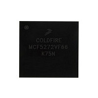
MCF5272VF66 Freescale, MCF5272VF66 Datasheet - Page 450

MCF5272VF66
Manufacturer Part Number
MCF5272VF66
Description
Manufacturer
Freescale
Datasheet
1.MCF5272VF66.pdf
(544 pages)
Specifications of MCF5272VF66
Family Name
MCF5xxx
Device Core
ColdFire
Device Core Size
32b
Frequency (max)
66MHz
Instruction Set Architecture
RISC
Supply Voltage 1 (typ)
3.3V
Operating Temp Range
0C to 70C
Operating Temperature Classification
Commercial
Mounting
Surface Mount
Pin Count
196
Package Type
MA-BGA
Lead Free Status / RoHS Status
Not Compliant
Available stocks
Company
Part Number
Manufacturer
Quantity
Price
Company:
Part Number:
MCF5272VF66
Manufacturer:
HYNIX
Quantity:
19
Company:
Part Number:
MCF5272VF66
Manufacturer:
FREESCAL
Quantity:
885
Company:
Part Number:
MCF5272VF66
Manufacturer:
Freescale Semiconductor
Quantity:
10 000
Part Number:
MCF5272VF66
Manufacturer:
FREESCALE
Quantity:
20 000
Company:
Part Number:
MCF5272VF66J
Manufacturer:
Freescale
Quantity:
256
Company:
Part Number:
MCF5272VF66J
Manufacturer:
Freescale Semiconductor
Quantity:
10 000
Company:
Part Number:
MCF5272VF66R2
Manufacturer:
Freescale Semiconductor
Quantity:
10 000
Company:
Part Number:
MCF5272VF66R2J
Manufacturer:
Freescale Semiconductor
Quantity:
10 000
- Current page: 450 of 544
- Download datasheet (7Mb)
Bus Operation
20.2.1
These output signals provide the location of a bus transfer. The address can be external SRAM, ROM,
FLASH, SDRAM, or peripherals.
20.2.2
These three-state bidirectional signals provide the general-purpose data path between the MCF5272 and
all other devices. The data bus can transfer 8, 16, 32, or 128 bits of data per bus transfer. The MCF5272
can be configured for an external physical data bus of 32- or 16-bits width. When configured for 16-bit
external data bus width, D[15:0] become GPIO port C. A write cycle drives all 32 or 16 bits of the data
bus regardless of the chip select port width and operand size.
20.2.3
This output signal defines the data transfer direction for the current bus cycle. A high (logic one) level
indicates a read cycle; a low (logic zero) level indicates a write cycle. During SDRAM bus cycles R/W is
driven high. When the CPU is in SLEEP or STOP modes, this signal is driven high.
20.2.4
This active-low synchronous input signal indicates the successful completion of a requested data transfer
operation. During MCF5272-initiated transfers, transfer acknowledge (TA) is an asynchronous input
signal from the referenced slave device indicating completion of the transfer.
The MCF5272 edge-detects and retimes the TA input. This means that an additional wait state may or may
not be inserted. For example if the active chip select is used to immediately generate the TA input, one or
two wait states may be inserted in the bus access.
The TA signal function is not available after reset. It must be enabled by configuring the appropriate pin
configuration register bits along with the value of CSORn[WS]. If TA is not used, it should either have a
pullup resistor or be driven through gating logic that always ensures the input is inactive. TA should be
negated on the negating edge of the active chip select.
20-2
Address Bus (A[22:0])
Data Bus (D[31:0])
Read/Write (R/W)
Transfer Acknowledge (TA)
The ColdFire core outputs 32 bits of address to the internal bus controller.
Of these 32 bits, only A[22:0] are output to pins on the MCF5272.
Use the OE signal to control any external data bus transceivers. In systems
containing numerous external peripherals, the chip selects should be used to
qualify any external transceivers. This ensures the transceivers are active
only when the desired peripheral is accessed. Using only the R/W signal to
control an external transceiver may lead to data bus conflicts in some system
architectures.
MCF5272 ColdFire
®
Integrated Microprocessor User’s Manual, Rev. 3
NOTE
NOTE
Freescale Semiconductor
Related parts for MCF5272VF66
Image
Part Number
Description
Manufacturer
Datasheet
Request
R
Part Number:
Description:
Mcf5272 Coldfire Integrated Microprocessor User
Manufacturer:
Freescale Semiconductor, Inc
Datasheet:

Part Number:
Description:
MCF5272 Interrupt Service Routine for the Physical Layer Interface Controller
Manufacturer:
Freescale Semiconductor / Motorola
Datasheet:

Part Number:
Description:
TOWER ELEVATOR BOARDS HARDWARE
Manufacturer:
Freescale Semiconductor
Datasheet:

Part Number:
Description:
TOWER SERIAL I/O HARDWARE
Manufacturer:
Freescale Semiconductor
Datasheet:

Part Number:
Description:
LCD MODULE FOR TWR SYSTEM
Manufacturer:
Freescale Semiconductor
Datasheet:

Part Number:
Description:
DAUGHTER LCD WVGA I.MX51
Manufacturer:
Freescale Semiconductor
Datasheet:

Part Number:
Description:
TOWER SYSTEM BOARD MPC5125
Manufacturer:
Freescale Semiconductor
Datasheet:

Part Number:
Description:
KIT EVALUATION I.MX51
Manufacturer:
Freescale Semiconductor
Datasheet:

Part Number:
Description:
KIT DEVELOPMENT WINCE IMX25
Manufacturer:
Freescale Semiconductor
Datasheet:

Part Number:
Description:
TOWER SYSTEM KIT MPC5125
Manufacturer:
Freescale Semiconductor
Datasheet:

Part Number:
Description:
TOWER SYSTEM BOARD K40X256
Manufacturer:
Freescale Semiconductor
Datasheet:

Part Number:
Description:
TOWER SYSTEM KIT K40X256
Manufacturer:
Freescale Semiconductor
Datasheet:

Part Number:
Description:
Microcontrollers (MCU) MX28 PLATFORM DEV KIT
Manufacturer:
Freescale Semiconductor
Datasheet:

Part Number:
Description:
MCU, MPU & DSP Development Tools IAR KickStart Kit for Kinetis K60
Manufacturer:
Freescale Semiconductor
Datasheet:

Part Number:
Description:
24BIT HDMI MX535/08
Manufacturer:
Freescale Semiconductor
Datasheet:


