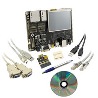
BMSKTOPASA900(DCE) Toshiba, BMSKTOPASA900(DCE) Datasheet - Page 935

BMSKTOPASA900(DCE)
Manufacturer Part Number
BMSKTOPASA900(DCE)
Description
KIT STARTER TMPA900 USB JTAG
Manufacturer
Toshiba
Series
TOPASr
Type
MCUr
Specifications of BMSKTOPASA900(DCE)
Contents
Evaluation Board, Cable(s), Software and Documentation
For Use With/related Products
TMPA900CMXBG
Lead Free Status / RoHS Status
Lead free / RoHS Compliant
- Current page: 935 of 959
- Download datasheet (5Mb)
Symbol
No.
4.3.2
VIX
10 CKE set-up time
11 Command set-up time
12 Command hold time
13 Data Setup Time
14 Data Hold Time
15 DMCDDM Setup Time
16 DMCDDM Hold Time
17
1 DMCDCLKP/ DMCDCLKN cycle time Note)
2 DMCDCLKP&DMCDCLKN Clock Skew time
3 CLK Differential Crosspoint cycle
4 CLK Differential Crosspoint cycle
5
6
7 DQS to Data Skew time
8 Address set-up time
9 Address hold time
DMCDQSx
Access time from CLK(CL* =3)
Data
Access time from CLK(CL* =3)
Write command to 1'st DQS Latching
Trasistion
AC Differential Cross point Voltage
DDR SDRAM Controller AC Electrical Characteristics
Note 1: Only DDR SDRAM devices of LVCMOS type are supported. DDR SDRAM devices of SSTIL (2.5 V) type are
Note 2: The “Equation” column in the table shows the specifications under the conditions DVCCM = 1.7 V to 1.9 V
*CL = CAS latency
Note: The internal bus cycle is T=10ns minimum value when the guaranteed temperature is 0 to 70 degree.
The internal bus cycle is T=13.3ns minimum value when the guaranteed temperature is -20 to 85 degree.
AC measurement conditions
• The letter “T” used in the equations in the table represents the period of internal bus frequency (f
• Output level: High = 0.7 × DVCCM, Low = 0.3 × DVCCM
•
• Clock output Differential level (VOD): VOD = 0.6 × DVCCM
• Clock output Differential Crosspoint level (VOX): High = 0.6 × DVCCM, Low = 0.4 × DVCCM
In case of DDR_SDRAM, CL number counting method is defferent with SDR_SDRAM.
Memory controller CL number = ( DDR_SDRAM’s CL Number ) – 1
which is one-half of the CPU clock (f
Input level: High = 0.9 × DVCCM, Low = 0.1 × DVCCM
not supported.
and DVCC1A = DVCC1B = DVCC1C = 1.4 to 1.6 V.
Parameter
Parameter
0.4 × DVCCM
TMPA900CM- 934
TENTATIVE
Min
Symbol
t
t
DQSQ
t
t
t
DQSS
t
t
CMS
CMH
t
t
t
t
t
t
CKS
t
t
t
AC1
AC2
CH
DH
MS
MH
CK
CL
AS
AH
DS
FCLK
).
0.25T - 1.5
0.25T - 1.5
0.25T - 1.5
0.25T - 1.5
0.5T - 3.0
0.5T - 0.5
0.5T - 0.5
0.5T - 3.0
0.5T - 3.0
0.5T - 3.0
0.5T - 3.0
0.75T
-0.35
Min
Typ.
T
0
Equation
2T-13.5
2T-13.5
1.25T
Max
0.35
0.6 × DVCCM
0.7
Max
7.50 to 12.5 7.80 to 13.0
MHz
100
4.5
4.5
6.5
6.5
0.7
2.0
2.0
2.0
2.0
2.0
1.0
1.0
1.0
1.0
10
Unit
MHz
10.4
96
4.7
4.7
7.3
7.3
0.7
2.2
2.2
2.2
2.2
2.2
1.1
1.1
1.1
1.1
1.7 ≤ DVCCM ≤ 1.9V
TMPA900CM
Condition
2009-10-14
Unit
ns
HCLK
),
Related parts for BMSKTOPASA900(DCE)
Image
Part Number
Description
Manufacturer
Datasheet
Request
R
Part Number:
Description:
Toshiba Semiconductor [TOSHIBA IGBT Module Silicon N Channel IGBT]
Manufacturer:
TOSHIBA Semiconductor CORPORATION
Datasheet:
Part Number:
Description:
TOSHIBA GTR MODULE SILICON NPN TRIPLE DIFFUSED TYPE
Manufacturer:
TOSHIBA Semiconductor CORPORATION
Datasheet:
Part Number:
Description:
TOSHIBA GTR Module Silicon N Channel IGBT
Manufacturer:
TOSHIBA Semiconductor CORPORATION
Datasheet:
Part Number:
Description:
TOSHIBA Intelligent Power Module Silicon N Channel IGBT
Manufacturer:
TOSHIBA Semiconductor CORPORATION
Datasheet:
Part Number:
Description:
TOSHIBA INTELLIGENT POWER MODULE SILICON N CHANNEL LGBT
Manufacturer:
TOSHIBA Semiconductor CORPORATION
Datasheet:
Part Number:
Description:
TOSHIBA IGBT Module Silicon N Channel IGBT
Manufacturer:
TOSHIBA Semiconductor CORPORATION
Datasheet:
Part Number:
Description:
TOSHIBA GTR MODULE SILICON N−CHANNEL IGBT
Manufacturer:
TOSHIBA Semiconductor CORPORATION
Datasheet:
Part Number:
Description:
TOSHIBA Intelligent Power Module Silicon N Channel IGBT
Manufacturer:
TOSHIBA Semiconductor CORPORATION
Datasheet:
Part Number:
Description:
TOSHIBA GTR Module Silicon N Channel IGBT
Manufacturer:
TOSHIBA Semiconductor CORPORATION
Datasheet:
Part Number:
Description:
TOSHIBA INTELLIGENT POWER MODULE
Manufacturer:
TOSHIBA Semiconductor CORPORATION
Datasheet:
Part Number:
Description:
TOSHIBA Intelligent Power Module Silicon N Channel IGBT
Manufacturer:
TOSHIBA Semiconductor CORPORATION
Datasheet:
Part Number:
Description:
TOSHIBA Intelligent Power Module Silicon N Channel IGBT
Manufacturer:
TOSHIBA Semiconductor CORPORATION
Datasheet:
Part Number:
Description:
TOSHIBA IGBT Module Silicon N Channel IGBT
Manufacturer:
TOSHIBA Semiconductor CORPORATION
Datasheet:
Part Number:
Description:
TOSHIBA Intelligent Power Module Silicon N Channel IGBT
Manufacturer:
TOSHIBA Semiconductor CORPORATION
Datasheet:
Part Number:
Description:
Toshiba Semiconductor [SILICON N CHANNEL 1GBT]
Manufacturer:
TOSHIBA Semiconductor CORPORATION
Datasheet:


