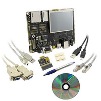
BMSKTOPASA900(DCE) Toshiba, BMSKTOPASA900(DCE) Datasheet - Page 302

BMSKTOPASA900(DCE)
Manufacturer Part Number
BMSKTOPASA900(DCE)
Description
KIT STARTER TMPA900 USB JTAG
Manufacturer
Toshiba
Series
TOPASr
Type
MCUr
Specifications of BMSKTOPASA900(DCE)
Contents
Evaluation Board, Cable(s), Software and Documentation
For Use With/related Products
TMPA900CMXBG
Lead Free Status / RoHS Status
Lead free / RoHS Compliant
- Current page: 302 of 959
- Download datasheet (5Mb)
[31:20]
[19:17]
[16:14]
[13:11]
[10:8]
[7:4]
[3:0]
[Description]
Bit
a. <t_tr>
b. <t_ pc>
c.
d. <t_ceoe>
e. <t_wc>
f.
• smc_sram_cycles0_x_5 (SMC SRAM Cycles Registers 0 <x>) (x = 0 to 3)
Note: This register cannot be read while it is in the Reset state.
5.
Turnaround time for SRAM chip configuration
0y000 to 0y111
Page cycle time:
0y000 to 0y111
<t_wp>
Delay time for smc_we_n_0:
0y000 to 0y111
Delay time for smc_oe_n_0:
0y000 to 0y111
Write cycle time
0y0000 to 0y1111
<t_rc>
Read cycle time
0y0000 to 0y1111
The structure and description of these registers are same as smc_sram_cycles0_0_5.
Please refer to the description of smc_sram_cycles0_0_5.
For the name and address of these registers, please refer to Table 3.10.11 MPMC1 SMC
SFR list.
−
t_tr
t_pc
t_wp
t_ceoe
t_wc
t_rc
smc_sram_cycles0_0_5 (SMC SRAM Cycles Registers 0 <0>)
Symbol
Bit
−
RO
RO
RO
RO
RO
RO
Type
TENTATIVE
TMPA900CM- 301
Undefined
0y001
0y010
0y110
0y011
0y1100
0y1100
Reset
Value
Read undefined.
Turnaround time for SRAM chip configuration
0y000 to 0y111
Page cycle time:
0y000 to 0y111
Delay time for smc_we_n_0:
0y000 to 0y111
Delay time for smc_oe_n_0:
0y000 to 0y111
Write cycle time:
0y0000 to 0y1111
Read cycle time:
0y0000 to 0y1111
Address = (0xF431_1000) + (0x0100)
Description
TMPA900CM
2009-10-14
Related parts for BMSKTOPASA900(DCE)
Image
Part Number
Description
Manufacturer
Datasheet
Request
R
Part Number:
Description:
Toshiba Semiconductor [TOSHIBA IGBT Module Silicon N Channel IGBT]
Manufacturer:
TOSHIBA Semiconductor CORPORATION
Datasheet:
Part Number:
Description:
TOSHIBA GTR MODULE SILICON NPN TRIPLE DIFFUSED TYPE
Manufacturer:
TOSHIBA Semiconductor CORPORATION
Datasheet:
Part Number:
Description:
TOSHIBA GTR Module Silicon N Channel IGBT
Manufacturer:
TOSHIBA Semiconductor CORPORATION
Datasheet:
Part Number:
Description:
TOSHIBA Intelligent Power Module Silicon N Channel IGBT
Manufacturer:
TOSHIBA Semiconductor CORPORATION
Datasheet:
Part Number:
Description:
TOSHIBA INTELLIGENT POWER MODULE SILICON N CHANNEL LGBT
Manufacturer:
TOSHIBA Semiconductor CORPORATION
Datasheet:
Part Number:
Description:
TOSHIBA IGBT Module Silicon N Channel IGBT
Manufacturer:
TOSHIBA Semiconductor CORPORATION
Datasheet:
Part Number:
Description:
TOSHIBA GTR MODULE SILICON N−CHANNEL IGBT
Manufacturer:
TOSHIBA Semiconductor CORPORATION
Datasheet:
Part Number:
Description:
TOSHIBA Intelligent Power Module Silicon N Channel IGBT
Manufacturer:
TOSHIBA Semiconductor CORPORATION
Datasheet:
Part Number:
Description:
TOSHIBA GTR Module Silicon N Channel IGBT
Manufacturer:
TOSHIBA Semiconductor CORPORATION
Datasheet:
Part Number:
Description:
TOSHIBA INTELLIGENT POWER MODULE
Manufacturer:
TOSHIBA Semiconductor CORPORATION
Datasheet:
Part Number:
Description:
TOSHIBA Intelligent Power Module Silicon N Channel IGBT
Manufacturer:
TOSHIBA Semiconductor CORPORATION
Datasheet:
Part Number:
Description:
TOSHIBA Intelligent Power Module Silicon N Channel IGBT
Manufacturer:
TOSHIBA Semiconductor CORPORATION
Datasheet:
Part Number:
Description:
TOSHIBA IGBT Module Silicon N Channel IGBT
Manufacturer:
TOSHIBA Semiconductor CORPORATION
Datasheet:
Part Number:
Description:
TOSHIBA Intelligent Power Module Silicon N Channel IGBT
Manufacturer:
TOSHIBA Semiconductor CORPORATION
Datasheet:
Part Number:
Description:
Toshiba Semiconductor [SILICON N CHANNEL 1GBT]
Manufacturer:
TOSHIBA Semiconductor CORPORATION
Datasheet:


