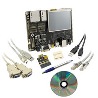
BMSKTOPASA900(DCE) Toshiba, BMSKTOPASA900(DCE) Datasheet - Page 462

BMSKTOPASA900(DCE)
Manufacturer Part Number
BMSKTOPASA900(DCE)
Description
KIT STARTER TMPA900 USB JTAG
Manufacturer
Toshiba
Series
TOPASr
Type
MCUr
Specifications of BMSKTOPASA900(DCE)
Contents
Evaluation Board, Cable(s), Software and Documentation
For Use With/related Products
TMPA900CMXBG
Lead Free Status / RoHS Status
Lead free / RoHS Compliant
- Current page: 462 of 959
- Download datasheet (5Mb)
• Serial frame (SP0FSS)
asserted during the entire transmission of the frame.
transmission of each frame. For this frame format, output data is transmitted on the rising
edge of SP0CLK, and input data is received on the falling edge.
• Microwire frame format
at half-duplex. In this mode, when a frame begins, an 8-bit control message is transmitted
to the slave. During this transmission, no incoming data is received by the SSP. After the
message has been sent, the slave decodes it and, after waiting one serial clock period after
the last bit of the 8-bit control message has been sent, responds with the requested data.
The returned data can be 4 to 16 bits in length, making the total frame length anywhere
from 13 to 25 bits.
SP0DO/SP0DI
For SPI and Microwire frame formats, the serial frame (SP0FSS) pin is active Low, and is
For SSI frame format, the SP0FSS pin is asserted for one bit rate period prior to the
The Microwire format uses a special master-slave messaging technique, which operates
The details of each frame format are described below.
SP0DO is put in the Hi-Z state whenever the SSP is idle. When data is written into the
transmit FIFO, the master pulses the SP0FSS line High for one SP0CLK period. The
transmit data is transferred from the transmit FIFO to the transmit serial shift
register. On the next rising edge of SP0CLK, the MSB of the 4 to 16-bit data frame is
shifted onto the SP0DO pin.
of SP0CLK. The received data is transferred from the serial shift register to the receive
FIFO on the first rising edge of SP0CLK after the LSB has been latched.
1) SSI frame format
SP0FSS
In this mode, SP0CLK and SP0FSS are forced Low and the transmit data line
Likewise, the MSB of the received data is input to the SP0DI pin on the falling edge
SSI frame format (single transfer)
SP0CLK
Hi-Z
TENTATIVE
TMPA900CM- 461
MSB
4 to16 bits
LSB
Hi-Z
TMPA900CM
2009-10-14
Related parts for BMSKTOPASA900(DCE)
Image
Part Number
Description
Manufacturer
Datasheet
Request
R
Part Number:
Description:
Toshiba Semiconductor [TOSHIBA IGBT Module Silicon N Channel IGBT]
Manufacturer:
TOSHIBA Semiconductor CORPORATION
Datasheet:
Part Number:
Description:
TOSHIBA GTR MODULE SILICON NPN TRIPLE DIFFUSED TYPE
Manufacturer:
TOSHIBA Semiconductor CORPORATION
Datasheet:
Part Number:
Description:
TOSHIBA GTR Module Silicon N Channel IGBT
Manufacturer:
TOSHIBA Semiconductor CORPORATION
Datasheet:
Part Number:
Description:
TOSHIBA Intelligent Power Module Silicon N Channel IGBT
Manufacturer:
TOSHIBA Semiconductor CORPORATION
Datasheet:
Part Number:
Description:
TOSHIBA INTELLIGENT POWER MODULE SILICON N CHANNEL LGBT
Manufacturer:
TOSHIBA Semiconductor CORPORATION
Datasheet:
Part Number:
Description:
TOSHIBA IGBT Module Silicon N Channel IGBT
Manufacturer:
TOSHIBA Semiconductor CORPORATION
Datasheet:
Part Number:
Description:
TOSHIBA GTR MODULE SILICON N−CHANNEL IGBT
Manufacturer:
TOSHIBA Semiconductor CORPORATION
Datasheet:
Part Number:
Description:
TOSHIBA Intelligent Power Module Silicon N Channel IGBT
Manufacturer:
TOSHIBA Semiconductor CORPORATION
Datasheet:
Part Number:
Description:
TOSHIBA GTR Module Silicon N Channel IGBT
Manufacturer:
TOSHIBA Semiconductor CORPORATION
Datasheet:
Part Number:
Description:
TOSHIBA INTELLIGENT POWER MODULE
Manufacturer:
TOSHIBA Semiconductor CORPORATION
Datasheet:
Part Number:
Description:
TOSHIBA Intelligent Power Module Silicon N Channel IGBT
Manufacturer:
TOSHIBA Semiconductor CORPORATION
Datasheet:
Part Number:
Description:
TOSHIBA Intelligent Power Module Silicon N Channel IGBT
Manufacturer:
TOSHIBA Semiconductor CORPORATION
Datasheet:
Part Number:
Description:
TOSHIBA IGBT Module Silicon N Channel IGBT
Manufacturer:
TOSHIBA Semiconductor CORPORATION
Datasheet:
Part Number:
Description:
TOSHIBA Intelligent Power Module Silicon N Channel IGBT
Manufacturer:
TOSHIBA Semiconductor CORPORATION
Datasheet:
Part Number:
Description:
Toshiba Semiconductor [SILICON N CHANNEL 1GBT]
Manufacturer:
TOSHIBA Semiconductor CORPORATION
Datasheet:


