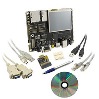
BMSKTOPASA900(DCE) Toshiba, BMSKTOPASA900(DCE) Datasheet - Page 466

BMSKTOPASA900(DCE)
Manufacturer Part Number
BMSKTOPASA900(DCE)
Description
KIT STARTER TMPA900 USB JTAG
Manufacturer
Toshiba
Series
TOPASr
Type
MCUr
Specifications of BMSKTOPASA900(DCE)
Contents
Evaluation Board, Cable(s), Software and Documentation
For Use With/related Products
TMPA900CMXBG
Lead Free Status / RoHS Status
Lead free / RoHS Compliant
- Current page: 466 of 959
- Download datasheet (5Mb)
SP0FSS
SP0CLK
SP0DO
SP0D I
Note: When the SSP of this microcontroller is used in slave mode, the SSP responds to every control data.
Note: When the SSP of this microcontroller is used in slave mode using Microwire frame format, the SSP responds
half-duplex instead of full-duplex, using master-slave data communications. In this
configuration, during idle periods:
SP0DO pin. During the transmission of 8-bit control data, the SP0FSS pin remains
Low and the SP0DI pin remains in the Hi-Z state.
After latching the last control bit, the slave device decodes the control byte during one
clock period and responds by transmitting data back to the SSP.
SP0CLK. The master SSP in turn latches each bit on the rising edge of SP0CLK. For
single transfers, the SP0FSS signal is pulled High one clock period after the last bit
has been latched by the master SSP.
3) Microwire frame format
to every control data because it has no capability to decode control data from the master. For this reason, the
SSP does not support multi-slave systems. When the SSP is used in master mode, it is not possible to
connect multiple slave devices. The SSP must always be used in a single-master, single-slave system.
Microwire frame format (single transfer)
Microwire format is very similar to SPI format, except that transmission is
• SP0CLK is forced Low
• SP0FSS is forced High
•the transmit data line SP0DO is undefined.
Data transmission is started by writing control data into the transmit FIFO.
The falling edge of SP0FSS causes the data in the transmit FIFO to be output on the
The off-chip slave device latches each control bit on each rising edge of SP0CLK.
Each bit of response data is driven onto the SP0DI line on the falling edge of
MSB
8 bit control data
TENTATIVE
TMPA900CM- 465
LSB
MSB
Output data
4 to 1 6 bit
LSB
TMPA900CM
2009-10-14
Related parts for BMSKTOPASA900(DCE)
Image
Part Number
Description
Manufacturer
Datasheet
Request
R
Part Number:
Description:
Toshiba Semiconductor [TOSHIBA IGBT Module Silicon N Channel IGBT]
Manufacturer:
TOSHIBA Semiconductor CORPORATION
Datasheet:
Part Number:
Description:
TOSHIBA GTR MODULE SILICON NPN TRIPLE DIFFUSED TYPE
Manufacturer:
TOSHIBA Semiconductor CORPORATION
Datasheet:
Part Number:
Description:
TOSHIBA GTR Module Silicon N Channel IGBT
Manufacturer:
TOSHIBA Semiconductor CORPORATION
Datasheet:
Part Number:
Description:
TOSHIBA Intelligent Power Module Silicon N Channel IGBT
Manufacturer:
TOSHIBA Semiconductor CORPORATION
Datasheet:
Part Number:
Description:
TOSHIBA INTELLIGENT POWER MODULE SILICON N CHANNEL LGBT
Manufacturer:
TOSHIBA Semiconductor CORPORATION
Datasheet:
Part Number:
Description:
TOSHIBA IGBT Module Silicon N Channel IGBT
Manufacturer:
TOSHIBA Semiconductor CORPORATION
Datasheet:
Part Number:
Description:
TOSHIBA GTR MODULE SILICON N−CHANNEL IGBT
Manufacturer:
TOSHIBA Semiconductor CORPORATION
Datasheet:
Part Number:
Description:
TOSHIBA Intelligent Power Module Silicon N Channel IGBT
Manufacturer:
TOSHIBA Semiconductor CORPORATION
Datasheet:
Part Number:
Description:
TOSHIBA GTR Module Silicon N Channel IGBT
Manufacturer:
TOSHIBA Semiconductor CORPORATION
Datasheet:
Part Number:
Description:
TOSHIBA INTELLIGENT POWER MODULE
Manufacturer:
TOSHIBA Semiconductor CORPORATION
Datasheet:
Part Number:
Description:
TOSHIBA Intelligent Power Module Silicon N Channel IGBT
Manufacturer:
TOSHIBA Semiconductor CORPORATION
Datasheet:
Part Number:
Description:
TOSHIBA Intelligent Power Module Silicon N Channel IGBT
Manufacturer:
TOSHIBA Semiconductor CORPORATION
Datasheet:
Part Number:
Description:
TOSHIBA IGBT Module Silicon N Channel IGBT
Manufacturer:
TOSHIBA Semiconductor CORPORATION
Datasheet:
Part Number:
Description:
TOSHIBA Intelligent Power Module Silicon N Channel IGBT
Manufacturer:
TOSHIBA Semiconductor CORPORATION
Datasheet:
Part Number:
Description:
Toshiba Semiconductor [SILICON N CHANNEL 1GBT]
Manufacturer:
TOSHIBA Semiconductor CORPORATION
Datasheet:


