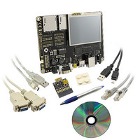
BMSKTOPASA900(DCE) Toshiba, BMSKTOPASA900(DCE) Datasheet - Page 771

BMSKTOPASA900(DCE)
Manufacturer Part Number
BMSKTOPASA900(DCE)
Description
KIT STARTER TMPA900 USB JTAG
Manufacturer
Toshiba
Series
TOPASr
Type
MCUr
Specifications of BMSKTOPASA900(DCE)
Contents
Evaluation Board, Cable(s), Software and Documentation
For Use With/related Products
TMPA900CMXBG
Lead Free Status / RoHS Status
Lead free / RoHS Compliant
- Current page: 771 of 959
- Download datasheet (5Mb)
1.
[31:20]
[19]
[18]
[17]
[16]
[15]
[14]
[13]
[12]
[11]
[10]
[9]
[8]
[7]
[6]
[5]
[4:1]
[0]
CMSCR (CMOS Image Sensor Control Register)
Bit
Note: Valid only when CMSCV<CCVM>[1] = 1.
−
Reserved
CSFOW
CSINTF
CFINTF
CSINTM
CFINTM
CDEDLY
CVSYPH
CHSYPH
CHBKPH
CPCKPH
CFOVF
CFDEF
CFPCLR
CINTSEL
CSIZE3:0
CSRST
Symbol
Bit
−
R/W
R/W
R/W
R/W
R/W
R/W
R/W
R/W
R/W
R/W
R/W
R/W
RO
WO
R/W
R/W
R/W
Type
Undefined
Undefined
0y0
0y0
0y0
0y0
0y0
0y0
0y0
0y0
0y0
0y0
0y0
0y0
0y0
0y0
0y0000
0y0
Reset
Value
TENTATIVE
TMPA900CM- 770
Read undefined. Write as zero.
Read undefined. Write as zero.
FIFO Read Window ”CMSFPT” switch
0y0: Use 4 bytes
0y1: Use 1 byte
CMOS sync interrupt flag
During READ
0y0: No interrupt
0y1: With interrupt
FIFO interrupt flag
During READ
0y0: No interrupt
0y1: With interrupt
CMOS sync interrupt mask setting
0y0: Interrupt masked
0y1: Interrupt enabled
FIFO interrupt mask setting
0y0: Interrupt masked
0y1: Interrupt enabled
Enable data delay function
0y0: Disable
0y1: Enable
VSYNC signal phase
0y0: Negative
0y1: Positive
HSYNC signal phase
0y0: Negative
0y1: Positive
HBK signal phase
0y0: Negative
0y1: Positive
PCK signal data capture edge select
0y0: Rise Up
0y1: Fall Down
FIFO Over Write Flag
During READ
0y0: No overwrite
0y1: No overwrite
FIFO Status Flag
0y0: No valid data
0y1: With valid data
FIFO pointer clear
0y0: Invalid
0y1: Clear *Note 1
CMOS sync interrupt generation timing setting
0y0: CMSVSY
0y1: CMSHBK
CMOS image sensor size (number of pixels) select
0y0000: QQVGA 0y0001: QVGA 0y0010: 320*180 0y0011: VGA
0y0100: Reserved 0y0101:4VGA
0y1000: CIF
0y1011 to 0y1111: Reserved
CMOS IS circuit reset
0y0: Invalid
0y1: Reset
0y1001: Reserved 0y1010:Reserved
During WRITE
0y0: Interrupt flag clear
0y1: Invalid
During WRITE
0y0: Interrupt flag clear
0y1: Invalid
During WRITE
0y0: Flag clear
0y1: Invalid
Address = (0xF202_0000) + (0x0000)
Description
0y0110SXGA
TMPA900CM
2009-10-14
0y0111: QCIF
Related parts for BMSKTOPASA900(DCE)
Image
Part Number
Description
Manufacturer
Datasheet
Request
R
Part Number:
Description:
Toshiba Semiconductor [TOSHIBA IGBT Module Silicon N Channel IGBT]
Manufacturer:
TOSHIBA Semiconductor CORPORATION
Datasheet:
Part Number:
Description:
TOSHIBA GTR MODULE SILICON NPN TRIPLE DIFFUSED TYPE
Manufacturer:
TOSHIBA Semiconductor CORPORATION
Datasheet:
Part Number:
Description:
TOSHIBA GTR Module Silicon N Channel IGBT
Manufacturer:
TOSHIBA Semiconductor CORPORATION
Datasheet:
Part Number:
Description:
TOSHIBA Intelligent Power Module Silicon N Channel IGBT
Manufacturer:
TOSHIBA Semiconductor CORPORATION
Datasheet:
Part Number:
Description:
TOSHIBA INTELLIGENT POWER MODULE SILICON N CHANNEL LGBT
Manufacturer:
TOSHIBA Semiconductor CORPORATION
Datasheet:
Part Number:
Description:
TOSHIBA IGBT Module Silicon N Channel IGBT
Manufacturer:
TOSHIBA Semiconductor CORPORATION
Datasheet:
Part Number:
Description:
TOSHIBA GTR MODULE SILICON N−CHANNEL IGBT
Manufacturer:
TOSHIBA Semiconductor CORPORATION
Datasheet:
Part Number:
Description:
TOSHIBA Intelligent Power Module Silicon N Channel IGBT
Manufacturer:
TOSHIBA Semiconductor CORPORATION
Datasheet:
Part Number:
Description:
TOSHIBA GTR Module Silicon N Channel IGBT
Manufacturer:
TOSHIBA Semiconductor CORPORATION
Datasheet:
Part Number:
Description:
TOSHIBA INTELLIGENT POWER MODULE
Manufacturer:
TOSHIBA Semiconductor CORPORATION
Datasheet:
Part Number:
Description:
TOSHIBA Intelligent Power Module Silicon N Channel IGBT
Manufacturer:
TOSHIBA Semiconductor CORPORATION
Datasheet:
Part Number:
Description:
TOSHIBA Intelligent Power Module Silicon N Channel IGBT
Manufacturer:
TOSHIBA Semiconductor CORPORATION
Datasheet:
Part Number:
Description:
TOSHIBA IGBT Module Silicon N Channel IGBT
Manufacturer:
TOSHIBA Semiconductor CORPORATION
Datasheet:
Part Number:
Description:
TOSHIBA Intelligent Power Module Silicon N Channel IGBT
Manufacturer:
TOSHIBA Semiconductor CORPORATION
Datasheet:
Part Number:
Description:
Toshiba Semiconductor [SILICON N CHANNEL 1GBT]
Manufacturer:
TOSHIBA Semiconductor CORPORATION
Datasheet:


