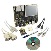
BMSKTOPASA900(DCE) Toshiba, BMSKTOPASA900(DCE) Datasheet - Page 699

BMSKTOPASA900(DCE)
Manufacturer Part Number
BMSKTOPASA900(DCE)
Description
KIT STARTER TMPA900 USB JTAG
Manufacturer
Toshiba
Series
TOPASr
Type
MCUr
Specifications of BMSKTOPASA900(DCE)
Contents
Evaluation Board, Cable(s), Software and Documentation
For Use With/related Products
TMPA900CMXBG
Lead Free Status / RoHS Status
Lead free / RoHS Compliant
- Current page: 699 of 959
- Download datasheet (5Mb)
[31:8]
[7]
[6]
[5]
[4]
[3]
[2]
[1]
[0]
STN64 gray
TFT16bit
others
STN64CR
Bit
Mode
Register
Name
3.19.4.2 Description of Registers
−
NoSpikeMode
CLFP_Inv
:CLLP_Inv
CLAC_Inv
LCP_Inv
G64_8bit
G64_en
Reserved
Note: When using STN 64-level grayscale mode, be sure to set LCLFP, LCLLP, LCLAC, and LCLCP identically with
Note1: For the LD bus switching mechanism, see Figure 3.19.5 LCDCOP Block Diagram LCDCOP Block Diagram.
Note2: For information about external 16-bit TFT signals, see Table3.19.6 LCD TFT panel signal multiplexing [TFT
1.
Symbol
0y1 :
Use STN 64 gray circuits
0y0 :
Not Use STN 64 gray circuits
0y0 :
Not Use STN 64 gray circuits
Bit
the settings in the LCDC.
16bit Interface]
STN64CR (LCDC Option Control Register)
0x0000
Address
The following lists the registers:
(base+)
<G64_en>
Table 3.19.9 The setting of STN 64 gray and TFT16 bit
−
R/W
R/W
R/W
R/W
R/W
R/W
R/W
R/W
Type
LCDC Option Control Register
Undefined
0y0
0y0
0y0
0y0
0y0
0y0
0y0
0y0
Reset
Value
Register setting
TENTATIVE
TMPA900CM- 698
Invert vertical synchronization(=VIS of CLCDC)
Invert horizontal synchronization (=HIS of CLCDC)
Invert output enable (= IOE of CLCDC)
0y0 : LCLAC output HIGH active in TFT mode
0y1 : LCLAC output LOW active in TFT mode
Invert panel clock (=IPC of CLCDC)
Read as undefined. Write as zero.
Delete noise of CLCP of LCDC
0y0 :
0y1 :
Read as undefined. Write as zero.
0y0 : LCLFP pin HIGH active
0y1 : LCLFP pin LOW active
0y0 : LCLLP pin HIGH active
0y0 : LCLCP rising edge
0y1 : LCLCP falling edge
Refer to the table of Table 3.19.9 The setting of STN 64 gray
and TFT16 bit .
0y1 : LCLLP pin LOW active
0y0 : External 4bit LD Bus
0y1 : External 8bit LD Bus
0y1 :
0y0 :
External LD12=CLD12
External LD6 =CLD6
External LD6 =CLD16
External LD12=CLD17
invalid
valid
<G64_8bit>
Description
Address = (0xF00B_0000) + (0x0000)
Description
Base address = 0xF00B_0000
If LD[15:0] Function of Port P
and Port V are setted,
<G64_8bit> need be seted to
0y1, to ouput CLD17, CLD16
Note
TMPA900CM
2009-10-14
Related parts for BMSKTOPASA900(DCE)
Image
Part Number
Description
Manufacturer
Datasheet
Request
R
Part Number:
Description:
Toshiba Semiconductor [TOSHIBA IGBT Module Silicon N Channel IGBT]
Manufacturer:
TOSHIBA Semiconductor CORPORATION
Datasheet:
Part Number:
Description:
TOSHIBA GTR MODULE SILICON NPN TRIPLE DIFFUSED TYPE
Manufacturer:
TOSHIBA Semiconductor CORPORATION
Datasheet:
Part Number:
Description:
TOSHIBA GTR Module Silicon N Channel IGBT
Manufacturer:
TOSHIBA Semiconductor CORPORATION
Datasheet:
Part Number:
Description:
TOSHIBA Intelligent Power Module Silicon N Channel IGBT
Manufacturer:
TOSHIBA Semiconductor CORPORATION
Datasheet:
Part Number:
Description:
TOSHIBA INTELLIGENT POWER MODULE SILICON N CHANNEL LGBT
Manufacturer:
TOSHIBA Semiconductor CORPORATION
Datasheet:
Part Number:
Description:
TOSHIBA IGBT Module Silicon N Channel IGBT
Manufacturer:
TOSHIBA Semiconductor CORPORATION
Datasheet:
Part Number:
Description:
TOSHIBA GTR MODULE SILICON N−CHANNEL IGBT
Manufacturer:
TOSHIBA Semiconductor CORPORATION
Datasheet:
Part Number:
Description:
TOSHIBA Intelligent Power Module Silicon N Channel IGBT
Manufacturer:
TOSHIBA Semiconductor CORPORATION
Datasheet:
Part Number:
Description:
TOSHIBA GTR Module Silicon N Channel IGBT
Manufacturer:
TOSHIBA Semiconductor CORPORATION
Datasheet:
Part Number:
Description:
TOSHIBA INTELLIGENT POWER MODULE
Manufacturer:
TOSHIBA Semiconductor CORPORATION
Datasheet:
Part Number:
Description:
TOSHIBA Intelligent Power Module Silicon N Channel IGBT
Manufacturer:
TOSHIBA Semiconductor CORPORATION
Datasheet:
Part Number:
Description:
TOSHIBA Intelligent Power Module Silicon N Channel IGBT
Manufacturer:
TOSHIBA Semiconductor CORPORATION
Datasheet:
Part Number:
Description:
TOSHIBA IGBT Module Silicon N Channel IGBT
Manufacturer:
TOSHIBA Semiconductor CORPORATION
Datasheet:
Part Number:
Description:
TOSHIBA Intelligent Power Module Silicon N Channel IGBT
Manufacturer:
TOSHIBA Semiconductor CORPORATION
Datasheet:
Part Number:
Description:
Toshiba Semiconductor [SILICON N CHANNEL 1GBT]
Manufacturer:
TOSHIBA Semiconductor CORPORATION
Datasheet:


