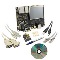
BMSKTOPASA900(DCE) Toshiba, BMSKTOPASA900(DCE) Datasheet - Page 811

BMSKTOPASA900(DCE)
Manufacturer Part Number
BMSKTOPASA900(DCE)
Description
KIT STARTER TMPA900 USB JTAG
Manufacturer
Toshiba
Series
TOPASr
Type
MCUr
Specifications of BMSKTOPASA900(DCE)
Contents
Evaluation Board, Cable(s), Software and Documentation
For Use With/related Products
TMPA900CMXBG
Lead Free Status / RoHS Status
Lead free / RoHS Compliant
- Current page: 811 of 959
- Download datasheet (5Mb)
1. ADREG0L (AD conversion result lower-order register 0
[31:8]
[7]
[6]
[5:2]
[1]
[0]
Bit
[Description]
• AD conversion result register.
a. <ADR0[1:0]>
b. <OVR0>
c. <ADR0RF>
R/W : Read/Write
Note : As ADREG0L to ADREG7L and ADREGSPL Registers are the same composition. Explain Register
higher-order/lower-order registers ADREG0H/L to ADREG7H/L. Top-priority conversion
results are stored in ADREGSPH/L. Since these registers are structured the same,
ADREG0 that is the conversion result storage register for the 0 channel is shown below:
They are AD conversion result lower-order bits 1 to 0.
Used for the overrun flag.
0y0: No overrun occurred
0y1: Overrun occurred
Used for the AD conversion result storage flag.
0y0: No change result
0y1: With conversion result
A/D conversion results are stored in the eight registers of A/D conversion result
−
ADR01
ADR00
−
OVR0
ADR0RF
About the address of ADREG1L to ADREG7L and ADREGSPL Register, please check Register Map.
ADREG0L only, the other Registers are same as ADREG0L.
Symbol
Bit
RO : Read Only
−
RO
RO
RO
RO
RO
Type
Undefined
0y0
0y0
0y0000
0y0
0y0
TENTATIVE
WO : Write Only
TMPA900CM- 810
Reset
Value
Read as undefined.
AD conversion result lower-order bit 1
AD conversion result lower-order bit 0
Always read as 0 when read.
Overrun flag
0y0: No overrun occurred
0y1: Overrun occurred
AD conversion result storage flag
0y0: No change result
0y1: With conversion result
Description
Address = (0xF008_0000) + (0x0040)
TMPA900CM
2009-10-14
Related parts for BMSKTOPASA900(DCE)
Image
Part Number
Description
Manufacturer
Datasheet
Request
R
Part Number:
Description:
Toshiba Semiconductor [TOSHIBA IGBT Module Silicon N Channel IGBT]
Manufacturer:
TOSHIBA Semiconductor CORPORATION
Datasheet:
Part Number:
Description:
TOSHIBA GTR MODULE SILICON NPN TRIPLE DIFFUSED TYPE
Manufacturer:
TOSHIBA Semiconductor CORPORATION
Datasheet:
Part Number:
Description:
TOSHIBA GTR Module Silicon N Channel IGBT
Manufacturer:
TOSHIBA Semiconductor CORPORATION
Datasheet:
Part Number:
Description:
TOSHIBA Intelligent Power Module Silicon N Channel IGBT
Manufacturer:
TOSHIBA Semiconductor CORPORATION
Datasheet:
Part Number:
Description:
TOSHIBA INTELLIGENT POWER MODULE SILICON N CHANNEL LGBT
Manufacturer:
TOSHIBA Semiconductor CORPORATION
Datasheet:
Part Number:
Description:
TOSHIBA IGBT Module Silicon N Channel IGBT
Manufacturer:
TOSHIBA Semiconductor CORPORATION
Datasheet:
Part Number:
Description:
TOSHIBA GTR MODULE SILICON N−CHANNEL IGBT
Manufacturer:
TOSHIBA Semiconductor CORPORATION
Datasheet:
Part Number:
Description:
TOSHIBA Intelligent Power Module Silicon N Channel IGBT
Manufacturer:
TOSHIBA Semiconductor CORPORATION
Datasheet:
Part Number:
Description:
TOSHIBA GTR Module Silicon N Channel IGBT
Manufacturer:
TOSHIBA Semiconductor CORPORATION
Datasheet:
Part Number:
Description:
TOSHIBA INTELLIGENT POWER MODULE
Manufacturer:
TOSHIBA Semiconductor CORPORATION
Datasheet:
Part Number:
Description:
TOSHIBA Intelligent Power Module Silicon N Channel IGBT
Manufacturer:
TOSHIBA Semiconductor CORPORATION
Datasheet:
Part Number:
Description:
TOSHIBA Intelligent Power Module Silicon N Channel IGBT
Manufacturer:
TOSHIBA Semiconductor CORPORATION
Datasheet:
Part Number:
Description:
TOSHIBA IGBT Module Silicon N Channel IGBT
Manufacturer:
TOSHIBA Semiconductor CORPORATION
Datasheet:
Part Number:
Description:
TOSHIBA Intelligent Power Module Silicon N Channel IGBT
Manufacturer:
TOSHIBA Semiconductor CORPORATION
Datasheet:
Part Number:
Description:
Toshiba Semiconductor [SILICON N CHANNEL 1GBT]
Manufacturer:
TOSHIBA Semiconductor CORPORATION
Datasheet:


