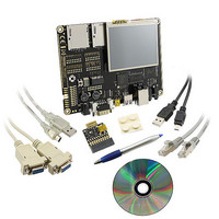
BMSKTOPASA900(DCE) Toshiba, BMSKTOPASA900(DCE) Datasheet - Page 775

BMSKTOPASA900(DCE)
Manufacturer Part Number
BMSKTOPASA900(DCE)
Description
KIT STARTER TMPA900 USB JTAG
Manufacturer
Toshiba
Series
TOPASr
Type
MCUr
Specifications of BMSKTOPASA900(DCE)
Contents
Evaluation Board, Cable(s), Software and Documentation
For Use With/related Products
TMPA900CMXBG
Lead Free Status / RoHS Status
Lead free / RoHS Compliant
- Current page: 775 of 959
- Download datasheet (5Mb)
CMSSCDMA
2.
Input Data
+Dummy8
RGB8:8:8
RGB8:8:8
RGB5:6:5
YUV4:2:2
Input Data
CMSYD
CMSUD
CMSVD
Format
・Data input from external pin (CMOS camera)
・Data Input from Internal Registers
Note : Dummy data is added only when the window of the FIFO buffer read register is configured to read 4 bytes of data at a
Format
[31:10]
[9]
[8:7]
[6]
[5]
[4:3]
[2]
[1:0]
Configure CRGBM and CCVM [1:0] according to the following table.
or
CMSCV (CMOS Image Sensor Color Space Conversion Register)
Bit
Note: When changing CMSCV<CCVM1:0>, keep CMSCR<CSRST>= 1 to be set.
time (CMCCR<CSFOW> = 0). Please note that dummy data is not added if CMCCR<CSFOW> = 1 (a byte of data
reading). Refer to 3.22.2.4 (4) “Formats of RGB Storage from FIFO buffer into the CMSFPT register” for details.
FIFO Output Format
FIFO Output Format
−
CSCVST
CSCVTRG[1:0]
CCVSMMS
CRGBM
CCVM[1:0]
DMAEN
−
Without Dummy
Without Dummy
Without Dummy
Without Dummy
Symbol
With Dummy
With Dummy
With Dummy
With Dummy
Bit
*Note 1
*Note 1
*Note
*Note
−
WO
R/W
R/W
R/W
R/W
R/W
−
Type
TENTATIVE
TMPA900CM- 774
FIFO Interrupt
Undefined
0y0
0y0
0y0
0y0
0y10
0y0
Undefined
FIFO interrupt
Water_Mark
Water_Mark
Reset
Value
32bytes
48bytes
32bytes
32bytes
32bytes
48bytes
32bytes
48bytes
Read undefined. Write as zero.
S/W conversion start
0y0: Invalid
0y1: Conversion start
S/W conversion start trigger select
(Enabled only when CCVM1 = 0y1 and CCVM0 = 0y0)
0y00: Write to CMSYD 0y01: Write to CMSUD
0y10: Write to CMSVD 0y11: Write 1 to <CSCVST>
Color space conversion factor mode select
0y0: Mode 1
0y1: Mode 2
RGB mode switching and FIFO Water Mark setting
Refer to the following table for details.
Color space conversion circuit input source
Refer to the following table for details.
DMA control
0y0: DMA request OFF
0y1: DMA request ON
Read undefined. Write as zero.
Output Data
Output Data
+Dummy8
RGB5:6:5
RGB8:8:8
RGB8:8:8
RGB8:8:8
RGB5:6:5
RGB5:6:5
RGB8:8:8
RGB5:6:5
RGB8:8:8
Format
Format
or
Description
Address = (0xF202_0000) + (0x0004)
CRGBM
CRGBM
0
1
1
0
0
1
0
1
CMSCV Register
CMSCV Register
Configuration
Configuration
CCVM1
CCVM1
TMPA900CM
0
0
0
0
1
1
1
1
2009-10-14
CCVM0
CCVM0
1
1
0
0
0
0
1
1
Related parts for BMSKTOPASA900(DCE)
Image
Part Number
Description
Manufacturer
Datasheet
Request
R
Part Number:
Description:
Toshiba Semiconductor [TOSHIBA IGBT Module Silicon N Channel IGBT]
Manufacturer:
TOSHIBA Semiconductor CORPORATION
Datasheet:
Part Number:
Description:
TOSHIBA GTR MODULE SILICON NPN TRIPLE DIFFUSED TYPE
Manufacturer:
TOSHIBA Semiconductor CORPORATION
Datasheet:
Part Number:
Description:
TOSHIBA GTR Module Silicon N Channel IGBT
Manufacturer:
TOSHIBA Semiconductor CORPORATION
Datasheet:
Part Number:
Description:
TOSHIBA Intelligent Power Module Silicon N Channel IGBT
Manufacturer:
TOSHIBA Semiconductor CORPORATION
Datasheet:
Part Number:
Description:
TOSHIBA INTELLIGENT POWER MODULE SILICON N CHANNEL LGBT
Manufacturer:
TOSHIBA Semiconductor CORPORATION
Datasheet:
Part Number:
Description:
TOSHIBA IGBT Module Silicon N Channel IGBT
Manufacturer:
TOSHIBA Semiconductor CORPORATION
Datasheet:
Part Number:
Description:
TOSHIBA GTR MODULE SILICON N−CHANNEL IGBT
Manufacturer:
TOSHIBA Semiconductor CORPORATION
Datasheet:
Part Number:
Description:
TOSHIBA Intelligent Power Module Silicon N Channel IGBT
Manufacturer:
TOSHIBA Semiconductor CORPORATION
Datasheet:
Part Number:
Description:
TOSHIBA GTR Module Silicon N Channel IGBT
Manufacturer:
TOSHIBA Semiconductor CORPORATION
Datasheet:
Part Number:
Description:
TOSHIBA INTELLIGENT POWER MODULE
Manufacturer:
TOSHIBA Semiconductor CORPORATION
Datasheet:
Part Number:
Description:
TOSHIBA Intelligent Power Module Silicon N Channel IGBT
Manufacturer:
TOSHIBA Semiconductor CORPORATION
Datasheet:
Part Number:
Description:
TOSHIBA Intelligent Power Module Silicon N Channel IGBT
Manufacturer:
TOSHIBA Semiconductor CORPORATION
Datasheet:
Part Number:
Description:
TOSHIBA IGBT Module Silicon N Channel IGBT
Manufacturer:
TOSHIBA Semiconductor CORPORATION
Datasheet:
Part Number:
Description:
TOSHIBA Intelligent Power Module Silicon N Channel IGBT
Manufacturer:
TOSHIBA Semiconductor CORPORATION
Datasheet:
Part Number:
Description:
Toshiba Semiconductor [SILICON N CHANNEL 1GBT]
Manufacturer:
TOSHIBA Semiconductor CORPORATION
Datasheet:


