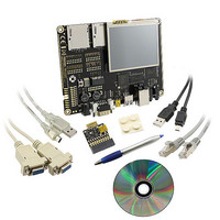
BMSKTOPASA900(DCE) Toshiba, BMSKTOPASA900(DCE) Datasheet - Page 922

BMSKTOPASA900(DCE)
Manufacturer Part Number
BMSKTOPASA900(DCE)
Description
KIT STARTER TMPA900 USB JTAG
Manufacturer
Toshiba
Series
TOPASr
Type
MCUr
Specifications of BMSKTOPASA900(DCE)
Contents
Evaluation Board, Cable(s), Software and Documentation
For Use With/related Products
TMPA900CMXBG
Lead Free Status / RoHS Status
Lead free / RoHS Compliant
- Current page: 922 of 959
- Download datasheet (5Mb)
4. CLKSMN (Lower detection frequency setting register)
5. CLKSMX (Higher detection frequency setting register)
[31:8]
[7:0]
[31:8]
[7:0]
<LDFS> and < HDFS >
[Explanation]
Bit
Bit
Note 1:
Note 2:
Note 3:
Note 4:
−
LDFS
−
HDFS
CLKSMN and CLKSMX cannot be written while the frequency detection operation is enabled
(CLKSCR2 = “0xE4”) or writing to the OFD registers is disabled (CLKSCR1="0x06").
CLKSMN and CLKSMX are protected from write operation by writing “0x06” to CLKSCR1. These
registers can be read regardless of the setting of CLKSCR1.
The values to be set to CLKSMN and CLKSMX should be determined depending on the clock
frequencies to be used to satisfy the condition CLKSMN < CLKSMX. For how to calculate the CLKSMN
and CLKSMX set values, see examples in 3.28.3 “Description of Operation”.
Otherwise the internal reset might be always assert into the CPU. (Deadlock state)
The setting of CLKSMN and CLKSMX should be set with enough safe including several percent error.
Symbol
Symbol
Bit
Bit
−
R/W
−
R/W
Type
Type
TMPA900CM - 921
Undefined
0xA5
Undefined
0xC9
TENTATIVE
Reset
Reset
Value
Value
Read undefined. Write as zero.
Read undefined. Write as zero.
Low detection frequency setting :
High detection frequency setting :
Description
Description
Address = (0xF009_0000)+(0x0020)
Address = (0xF009_0000)+(0x0010)
TMPA900CM
2009-10-14
Related parts for BMSKTOPASA900(DCE)
Image
Part Number
Description
Manufacturer
Datasheet
Request
R
Part Number:
Description:
Toshiba Semiconductor [TOSHIBA IGBT Module Silicon N Channel IGBT]
Manufacturer:
TOSHIBA Semiconductor CORPORATION
Datasheet:
Part Number:
Description:
TOSHIBA GTR MODULE SILICON NPN TRIPLE DIFFUSED TYPE
Manufacturer:
TOSHIBA Semiconductor CORPORATION
Datasheet:
Part Number:
Description:
TOSHIBA GTR Module Silicon N Channel IGBT
Manufacturer:
TOSHIBA Semiconductor CORPORATION
Datasheet:
Part Number:
Description:
TOSHIBA Intelligent Power Module Silicon N Channel IGBT
Manufacturer:
TOSHIBA Semiconductor CORPORATION
Datasheet:
Part Number:
Description:
TOSHIBA INTELLIGENT POWER MODULE SILICON N CHANNEL LGBT
Manufacturer:
TOSHIBA Semiconductor CORPORATION
Datasheet:
Part Number:
Description:
TOSHIBA IGBT Module Silicon N Channel IGBT
Manufacturer:
TOSHIBA Semiconductor CORPORATION
Datasheet:
Part Number:
Description:
TOSHIBA GTR MODULE SILICON N−CHANNEL IGBT
Manufacturer:
TOSHIBA Semiconductor CORPORATION
Datasheet:
Part Number:
Description:
TOSHIBA Intelligent Power Module Silicon N Channel IGBT
Manufacturer:
TOSHIBA Semiconductor CORPORATION
Datasheet:
Part Number:
Description:
TOSHIBA GTR Module Silicon N Channel IGBT
Manufacturer:
TOSHIBA Semiconductor CORPORATION
Datasheet:
Part Number:
Description:
TOSHIBA INTELLIGENT POWER MODULE
Manufacturer:
TOSHIBA Semiconductor CORPORATION
Datasheet:
Part Number:
Description:
TOSHIBA Intelligent Power Module Silicon N Channel IGBT
Manufacturer:
TOSHIBA Semiconductor CORPORATION
Datasheet:
Part Number:
Description:
TOSHIBA Intelligent Power Module Silicon N Channel IGBT
Manufacturer:
TOSHIBA Semiconductor CORPORATION
Datasheet:
Part Number:
Description:
TOSHIBA IGBT Module Silicon N Channel IGBT
Manufacturer:
TOSHIBA Semiconductor CORPORATION
Datasheet:
Part Number:
Description:
TOSHIBA Intelligent Power Module Silicon N Channel IGBT
Manufacturer:
TOSHIBA Semiconductor CORPORATION
Datasheet:
Part Number:
Description:
Toshiba Semiconductor [SILICON N CHANNEL 1GBT]
Manufacturer:
TOSHIBA Semiconductor CORPORATION
Datasheet:


