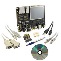
BMSKTOPASA900(DCE) Toshiba, BMSKTOPASA900(DCE) Datasheet - Page 932

BMSKTOPASA900(DCE)
Manufacturer Part Number
BMSKTOPASA900(DCE)
Description
KIT STARTER TMPA900 USB JTAG
Manufacturer
Toshiba
Series
TOPASr
Type
MCUr
Specifications of BMSKTOPASA900(DCE)
Contents
Evaluation Board, Cable(s), Software and Documentation
For Use With/related Products
TMPA900CMXBG
Lead Free Status / RoHS Status
Lead free / RoHS Compliant
- Current page: 932 of 959
- Download datasheet (5Mb)
No.
4.3
10
11
12
13
14
15
1
2
3
4
5
6
7
8
9
4.3.1
Measuring Condition
Loaded capacitance
Internal bus period ( = T)
A0-A23 valid to D0-D31 input
SMCOEn fall to D0-D31 input
SMCOEn low level pulse width
A0-A23 valid to SMCOEn fall
SMCOEn rise to D0-D31 hold
SMCOEn high level pulse width
D0-D31 valid to SMCWEn rise
D0-D31 valid to SMCWEn rise (bls=1)
SMCWEn low level width
A0-A23 valid to SMCWEn fall
SMCWEn rise to A0-A23 hold
SMCWEn rise to D0-D31 hold
SMCOEn rise to D0-D31 output
Data byte control to write complete time
All AC specifications shown below are the measurement results under the following conditions
unless specified otherwise.
AC Electrical Characteristics
Connection
Software configuration
Note: The “Equation” column in the table shows the specifications under the conditions DVCCM
Note: The internal bus cycle is T=10ns minimum value when the guaranteed temperature is 0 to 70 degree.
The internal bus cycle is T=13.3ns minimum value when the guaranteed temperature is -20 to 85 degree.
AC measurement conditions
• The letter “T” used in the equations in the table represents the period of internal bus frequency (f
• Output level: High = 0.7 × DVCCM, Low = 0.3 × DVCCM
• Input level: High = 0.9 × DVCCM, Low = 0.1 × DVCCM
•
Basic Bus Cycles
CL = 25 pF
Read cycle (asynchronous mode)
Write cycle (asynchronous mode)
which is one-half of the CPU clock (f
The variables used in the equations in the table are defined as follows:
DVCCM
1. DVCC3IO × 0.7 ≤ SELDVCCM ≤ DVCC3IO
1. PMCDRV<DRV_MEM1:0> = 0y11 (Full Drive at 1.8±0.1V)
2. PMCDRV<DRV_MEM1:0> = 0y01 (Half Drive at 3.3±0.3V)
Parameter
=
3.0 V to 3.6 V and DVCC1A
Note)
N = Number of t
K = Number of t
WC
RC
cycles
cycles
TMPA900CM- 931
TENTATIVE
Symbol
t
t
OEHW
t
t
t
t
t
t
t
OEW
t
t
OED
t
t
OEO
SBW
CYC
t
AOE
t
SDS
WW
DW
WA
WD
AW
AD
HR
=
FCLK
DVCC1B
).
(N-M)T – 10.0
(K-L-1)T – 5.0
(K-L-1)T – 5.0
(L+1)T – 10.0
(L+1)T – 10.0
(N-M)T – 8.0
(N)T – 15.0
MT – 5.0
MT – 8.0
LT – 8.0
LT – 8.0
M = Number of t
L = Number of t
=
T – 5.0
Min
DVCC1C
10
0
2
Equation
=
1.4 to 1.6 V.
WP
Max
CEOE
800
cycles
cycles
100 MHz
N=10
K=10
M=3
10.0
85.0
60.0
62.0
60.0
60.0
52.0
25.0
25.0
52.0
L=6
5.0
2.0
25
22
0
96 MHz
N=10
K=10
M=3
10.4
89.2
62.8
64.9
26.3
23.3
62.9
62.9
54.5
26.3
26.3
54.5
L=6
5.4
2.0
=
0
1.7 V to 1.9 V or
TMPA900CM
2009-10-14
48 MHz
N=5
M=1
20.8
89.2
73.3
75.3
15.8
12.8
73.3
73.3
15.8
15.8
15.8
54.5
K=5
L=3
2.0
54
0
HCLK
Unit
)
ns
ns
Related parts for BMSKTOPASA900(DCE)
Image
Part Number
Description
Manufacturer
Datasheet
Request
R
Part Number:
Description:
Toshiba Semiconductor [TOSHIBA IGBT Module Silicon N Channel IGBT]
Manufacturer:
TOSHIBA Semiconductor CORPORATION
Datasheet:
Part Number:
Description:
TOSHIBA GTR MODULE SILICON NPN TRIPLE DIFFUSED TYPE
Manufacturer:
TOSHIBA Semiconductor CORPORATION
Datasheet:
Part Number:
Description:
TOSHIBA GTR Module Silicon N Channel IGBT
Manufacturer:
TOSHIBA Semiconductor CORPORATION
Datasheet:
Part Number:
Description:
TOSHIBA Intelligent Power Module Silicon N Channel IGBT
Manufacturer:
TOSHIBA Semiconductor CORPORATION
Datasheet:
Part Number:
Description:
TOSHIBA INTELLIGENT POWER MODULE SILICON N CHANNEL LGBT
Manufacturer:
TOSHIBA Semiconductor CORPORATION
Datasheet:
Part Number:
Description:
TOSHIBA IGBT Module Silicon N Channel IGBT
Manufacturer:
TOSHIBA Semiconductor CORPORATION
Datasheet:
Part Number:
Description:
TOSHIBA GTR MODULE SILICON N−CHANNEL IGBT
Manufacturer:
TOSHIBA Semiconductor CORPORATION
Datasheet:
Part Number:
Description:
TOSHIBA Intelligent Power Module Silicon N Channel IGBT
Manufacturer:
TOSHIBA Semiconductor CORPORATION
Datasheet:
Part Number:
Description:
TOSHIBA GTR Module Silicon N Channel IGBT
Manufacturer:
TOSHIBA Semiconductor CORPORATION
Datasheet:
Part Number:
Description:
TOSHIBA INTELLIGENT POWER MODULE
Manufacturer:
TOSHIBA Semiconductor CORPORATION
Datasheet:
Part Number:
Description:
TOSHIBA Intelligent Power Module Silicon N Channel IGBT
Manufacturer:
TOSHIBA Semiconductor CORPORATION
Datasheet:
Part Number:
Description:
TOSHIBA Intelligent Power Module Silicon N Channel IGBT
Manufacturer:
TOSHIBA Semiconductor CORPORATION
Datasheet:
Part Number:
Description:
TOSHIBA IGBT Module Silicon N Channel IGBT
Manufacturer:
TOSHIBA Semiconductor CORPORATION
Datasheet:
Part Number:
Description:
TOSHIBA Intelligent Power Module Silicon N Channel IGBT
Manufacturer:
TOSHIBA Semiconductor CORPORATION
Datasheet:
Part Number:
Description:
Toshiba Semiconductor [SILICON N CHANNEL 1GBT]
Manufacturer:
TOSHIBA Semiconductor CORPORATION
Datasheet:


